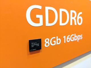
SK Hynix Showcases GDDR6 AT GTC

SK Hynix is displaying its next generation GDDR6 memory modules at Nvidia's GTC event in San Jose, California. According to the memory maker, GDDR6 operates with an I/O data rate of 16Gbps and a theoretical bandwidth of 768GB/s when paired with a 384-bit I/O bus. This new memory standard allows for twice the bandwidth per pin as GDDR5 and delivers 10% lower power consumption. It is expected to power Nvidia's upcoming Volta GPU architecture.

SK Hynix is the world’s second-largest memory chipmaker and world’s fifth largest semiconductor company. Just a few short weeks ago, senior vice president Jonghoon Oh, the Head of SK Hynix's DRAM Product Development Division said in a press release:
“With the introduction of this industry’s fastest GDDR6, SK Hynix will actively respond to high quality, high-performance graphics memory solutions market. The Company would help our clients enhance their performance of high-end graphics cards,” he added.
According to SK Hynix, the company has been collaborating with “a core graphics chipset client” to mass produce the GDDR6 for the upcoming market demands.
Putting these numbers into perspective, standard GDDR5 offers 8 Gbps of throughput, GDDR5X memory offers up to 12 Gbps, and GDDR6 offers speeds up to 16 Gbps. Here's a comparison list of GDDR5 versus GDDR6:
| Row 0 - Cell 0 | GDDR5 | GDDR6 |
| Density | 4GB ~ 8Gb | 8Gb ~ 16Gb |
| Package | 170B (12x14) 0.8mm pitch | 180B (12x14) 0.75mm pitch |
| Burst Length | 8bit (DDR) | 16bit (DDR/QDR optional) |
| External IO | X32 (x16) | 2CH x32 (2CH x16 & PC Mode x32) |
| WCK Granularity | byte | Byte / word (optional) |
| Pre-fetch per CH | 256bit (32GB access) | 256bit (32B) |
| WCK Rate | 2f (DDR) | 4f (DDR) / 2f (QDR) |
| Pin Data Rate | 8Gbps (Target 10Gbps) | Up to 16Gbps |
| IO | POD | POD |
| Voltage | 1.5V (1.35V) | 1.35V |
| VPP | - | 1.8V |
| Rx | CTLE per word | 1-tap DFE per DQ |
| CA Training @SRF | NO | YES |
| EDC Rate | Full (0x83 72bit) | Full / Half (0x83 144bit / 0x83 XOR) |
Stay on the Cutting Edge
Join the experts who read Tom's Hardware for the inside track on enthusiast PC tech news — and have for over 25 years. We'll send breaking news and in-depth reviews of CPUs, GPUs, AI, maker hardware and more straight to your inbox.
-
bit_user Reply
Yes. This is no comparison to HBM2.19674679 said:No comparison to HBM2?
; )
The problem with ever-faster DDR standards is that latency tends to increase faster than bandwidth.
HBM2 is interesting because it's:■ higher-bandwidth
■ lower-power
■ lower-latencyEventually, it might even be cheaper, since it'll save on board traces & manufacturing costs. -
palladin9479 Reply19675550 said:
Yes. This is no comparison to HBM2.19674679 said:No comparison to HBM2?
; )
The problem with ever-faster DDR standards is that latency tends to increase faster than bandwidth.
HBM2 is interesting because it's:■ higher-bandwidth
■ lower-power
■ lower-latencyEventually, it might even be cheaper, since it'll save on board traces & manufacturing costs.
The Bandwidth vs Latency have increased identical to each other. 7ns is the floor for traditional DRAM models because the signal needs to reach the end of the bus before a new signal can by put on that bus. Each of the chips on a DRAM channel on chained together and the more DRAM chips you have on a bus the longer the buffer time on the signal. This is why 2x2 configurations have better performance then 2x4 configurations with the same quality chips, half the chips per channel means less time needed for the signal to terminate and tighter timings. SDR through DDR3 kept the same general topology with various minor adjustments, GDDR memories were just their system counterparts with specialized topology for a greatly expanded number of individual ranks and bus's. HBM just takes the GDDR concept and amplifies it to an obscene level.
And here is where the problem begins, large wide configurations have lower clock rates then small narrow configurations. This results in them having longer latencies because physics (giant discussion here if you want). Both GDDR and HBM have really high command latencies, usually 3~10x what a piece of DDR would have. In the graphics world this is fine because a GPU's vector workload is so paralleled that feeding massive quantities of data is more important then waiting on a single command's return, their entire design is around buffering a ton of data and sending it in a torrent to the cores for calculation, once the torrent starts up it doesn't stop. In contrast a system CPU needs to constantly alter and adjust it's data stream based on the results of a previous instruction, this makes the ability to rapidly respond to commands more important then having a vast data torrent pouring in.
Short version, for GPU's Bandwidth >>> Latency, for CPU's Real Latency >>> Bandwidth. That is why we use different memory technologies for each. -
Joe Black GDDR I believe is for mainstream parts and will continue to be. The HBM moniker will be restricted to enthusiast cards.Reply -
hannibal HBM is for enterprize calculation cards for Nvidia. Amd will use HBM in highend consumer cards. Hopefully amd Also goes back to gddr in their cards too... cheaper cards, with allmost the same speed.Reply
Most Popular


