Comparison: T-Bred "B" Vs. T-Bred "A" Vs. Palomino, Continued

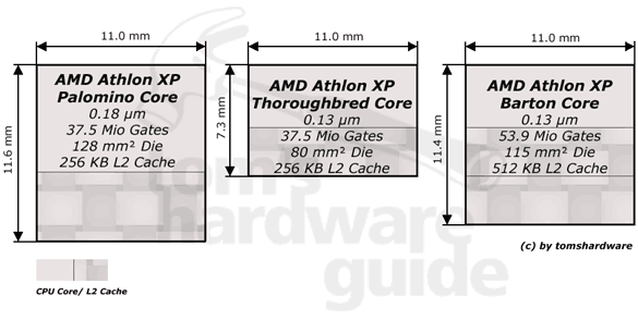
With the launch of the Thoroughbred core in the "B" version, AMD Athlon reaches the fourth level in its evolution. The first core, the Thunderbird, was introduced about two years ago. AMD made a further step in October 2001 by introducing the Palomino core, which essentially consisted of the SSE command set expansion and an optimization of the cache line. The Thoroughbred core has been around since June 2002, and this one involves a rearrangement of the CPU's internal components, as well as smaller structures (0.13 micron). In order to give you a complete picture, we've included the data for the Barton core, which is expected to be out in Q3. The Barton represents the fifth and last level of development of the Athlon program, based on Socket 462.
| Manufacturer | AMD | AMD | AMD | AMD | Intel |
|---|---|---|---|---|---|
| Processor | Athlon XPThoroughbred "B" Core | Athlon XPThoroughbred Core "A" Core | Athlon XPPalomino Core | AthlonThunderbird Core | Pentium 4Northwood Core |
| Introduction | Q3, 2002 | Q2, 2002 | October 9, 2001 | October 9, 2001 | January 7, 2002 |
| Clock Frequencies | 1.86 - 2.66 GHz | 1.46 - 1.80 GHz | 1.2 - 1.80 GHz | 0.65 - 1.40 GHz | 1.6 - 3.06 GHz |
| Manufacturing Process | 0,13 µm | 0,13 µm | 0,18 µm | 0,18 µm | 0,13 µm |
| Die size | 84 mm2 | 80 mm2 | 128 mm2 | 128 mm2 | 146 mm2 |
| Number of Gates | 37,5 Million | 37,5 Million | 37,5 Million | 37,5 Million | 55 Million |
| Platform | Socket462 | Socket462 | Socket462 | Socket462 | Socket478 |
| CPU Bus Clock (Front Side Bus) | 133 MHz266 MHz DDR | 133 MHz266 MHz DDR | 133 MHz266 MHz DDR | 100/133 MHz200/266 MHz DDR | 100/133 MHz400/533 MHz QDR |
| L1 Execution Cache Size | 64 kB | 64 kB | 64 kB | 64 kB | 12.000 µ-Ops (Trace Cache) |
| Execution Pre Decode? | no | no | no | no | yes |
| L1 Data Cache Size | 64 kB | 64 kB | 64 kB | 64 kB | 8 kB (unconfirmed) |
| Hardware Data Prefetch | yes | yes | yes | yes | yes |
| L1 Cache Clock | core clock | core clock | core clock | core clock | core clock |
| L1 Data Cache Bus Width | 64 bit | 64 bit | 64 bit | 64 bit | 256 bit |
| L2 Cache Size | 256 kB | 256 kB | 256 kB | 256 kB | 512 kB |
| L2 Cache Clock | core clock | core clock | core clock | core clock | core clock |
| L2 Cache Addressable Range | 64 GB | 64 GB | 64 GB | 64 GB | 64 GB |
| Processor Data Bus Width | 64 bit | 64 bit | 64 bit | 64 bit | 64 bit |
| Platform Support | |||||
| Chipsets | VIA KT333 to KT400SiS 735 and SiS 745Nvidia nForce, nForce 2AMD 750 and 760 | VIA KT133A to KT400SiS 735 and SiS 745ALi Magik 1Nvidia nForce, nForce 2AMD 750 and 760 | VIA KT133 to KT400SiS 735 and SiS 745ALi Magik 1Nvidia nForce, nForce 2AMD 750 and 760 | VIA KT133 to KT400SiS 735 and SiS 745ALi Magik 1Nvidia nForce, nForce 2AMD 750 and 760 | Intel i845, Intel i845D, Intel i845E, i845G, i845EG, i845EPIntel i850 and Intel i850EVIA P4X266, VIA P4X266AVIA P4X333, VIA P4X400SiS 645, SiS 645DX, SiS 648 |
| Type of Memory | SDRAMDDR-SDRAM | SDRAMDDR-SDRAM | SDRAMDDR-SDRAM | SDRAMDDR-SDRAM | SDRAMDDR-SDRAM, RDRAM |
| Memory Clock | 100/133/166/200 MHz | 100/133/166/200 MHz | 100/133/166 MHz | 100/133/166 MHz | 100/133/166/300/400/533 MHz |
| Instruction Extensions | |||||
| MMX | yes | yes | yes | yes | yes |
| Enhanced 3DNow! | yes | yes | yes | yes | no |
| 3DNow! Professional | yes | yes | yes | yes | no |
| SSE | yes | yes | yes | yes | yes |
| SSE2 | no | no | no | no | yes |
| Electrical Specifications | |||||
| SMP-Support | no ('not officially endorsed or supported') | no ('not officially endorsed or supported') | no ('not officially endorsed or supported') | no ('not officially endorsed or supported') | no |
| Core Voltage | 1,65 Volt | 1,65 Volt | 1,75 Volt | 1,75 Volt | 1,5 Volt |
| Thermal Protection (Thermal Diode) | yes | yes | yes | yes | yes |
| Integrated Thermal Protection Logic | no, requires logic on motherboard | no, requires logic on motherboard | no, requires logic on motherboard | no, requires logic on motherboard | yes |


