VIA's Offering For The AMD Hammer
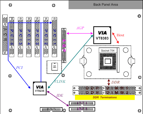
Overview of the structure of the VIA reference board, including the connections between the individual components.
Most likely, AMD will launch the ClawHammer for the desktop market at CeBIT 2003. In the beginning, there will be a platform with a chipset combination consisting of the AMD 8151 Northbridge and the Ali Southbridge. The technically outmoded Southbridge, the AMD 8111, only offers USB 1.1 support, which is why another chip was needed for the USB 2.0 functionality. In general, motherboard manufacturers are refraining from using a combination of the two AMD chips and turning instead to solutions from VIA, NVIDIA and ATI. At the moment, it's not quite clear yet whether or not the Taiwanese manufacturer SiS will be sitting in the same boat.
The following differences are to be found between the individual chips: with VIA, communication between the Northbridge and Southbridge will occur through V-Link-533. By contrast, there's the pure AMD solution, which is the combination of AMD Northbridge and Southbridge that uses Hypertransport protocol (533). Note: the two protocols are not compatible to one another. However the Hammer CPU exchanges data with the Northbridge via Hypertransport at 1600 MB/s. VIA offers a total of three different chipsets for the Socket 754 platform: the K8T400, K8T400M and K8M400, which are simpler models with integrated graphics.
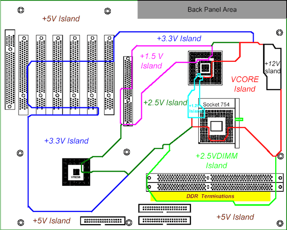
The various voltage areas on the motherboard.

Motherboard layout for the first layer.

Motherboard layout for printing.
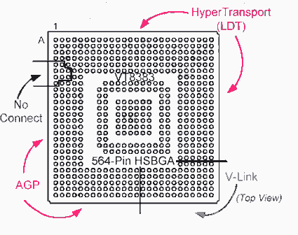
The division of the individual pins on the VIA Northbridge (underside).
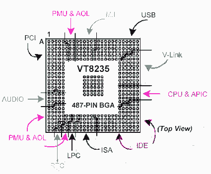
The division of the individual pins on the VIA Southbridge (underside).
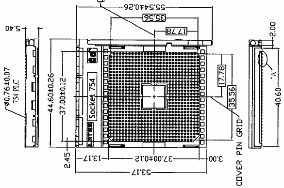
The dimensions of Socket 754.


