Intel's 45 nm Penryn CPU: 4 GHz Air Cooled
45 nm - Higher Yield, Smaller Die Area
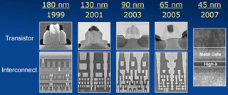
Like clockwork, Intel shrinks the structures of its processors every two years, and has already planned ahead as far as 2009. While 45 nm processors are only now set to enter the channel, the first prototypes of chips built on a 32 nm process are being tested in Intel's labs.

Beginning with the 45 nm technology, new materials need to be investigated that can be used in the production process. While it has thus far been possible to use the practically same materials across a variety of different processes, a new material now needs to be found for such small structures.
The 45 nm production process offers the following advantages over the 65 nm process:
- Almost twice as many transistors can fit onto the same chip area.
- Power consumption is reduced by about 30%.
This is in line with "Moore's Law", the prediction originally made by Gordon Moore that states that the number of transistors roughly doubles with each process generation.

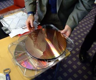
At Intel's press event in Munich, each of the journalists present had the opportunity to hold a 300 mm wafer in his hands.

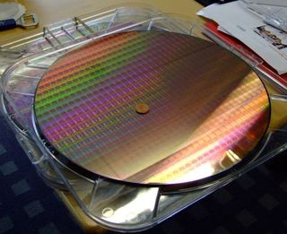
300 mm wafer with Penryn cores.

The Penryn core is smaller than a penny.
Stay on the Cutting Edge
Join the experts who read Tom's Hardware for the inside track on enthusiast PC tech news — and have for over 25 years. We'll send breaking news and in-depth reviews of CPUs, GPUs, AI, maker hardware and more straight to your inbox.
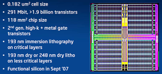
Intel's research on 32 nm structures is in full swing. Functional SRAM chips have been running in Intel's labs since September of this year.

Current page: 45 nm - Higher Yield, Smaller Die Area
Prev Page New Dielectric Minimizes Leakage Currents Next Page 12 MB L2 Cache And SSE 4Tom's Hardware's dedicated news crew consists of both freelancers and staff with decades of experience reporting on the latest developments in CPUs, GPUs, super computing, Raspberry Pis and more.
Most Popular


