Manufacturing Process
The process of manufacturing a PCB starts with a board of Glass Epoxy or similar substrate. This is referred to as the base substrate.
Imaging (Forming The Conductor Pattern)
The first step is to create the conductor pattern that provides the electrical connection between the components. We will here give an introduction to a 'Subtractive transfer' of the artwork into metal conductors. This technique involves covering the whole base substrate with a thin copper film and then remove the superfluous copper. 'Additive PatternTtransfer' is another less common way of creating the conductors. The copper is then only added where the wires are to be formed. We will not discuss Additive Pattern Transfer in more detail here.
If a double-sided PCB is to be made, the base substrate is covered on both sides with the copper film. For multi-layer PCBs several of these boards are made and laminated together at a later stage.
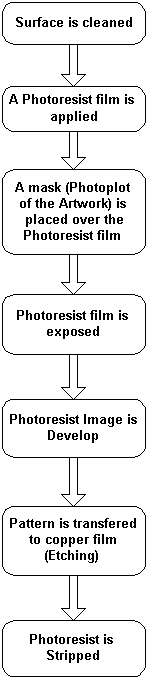
The following flowchart shows how the conductor pattern is formed on the base substrate.