R600: Finally DX10 Hardware from ATI
Memory Interface And Distribution
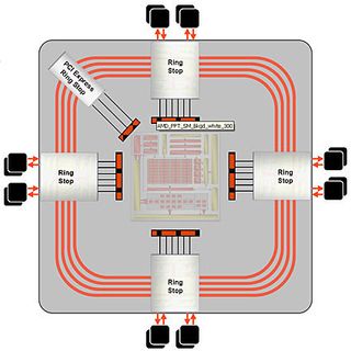
If you recall when ATI launched R520 (X1900), you will remember that it introduced a new memory bus in the form of a ring. Most chip designs and even ATI's previous generations used centralized crossbars, which inherently are a good design. There is, however, a serious drawback as the design scales up the number of clients it served (n^2 to be exact). It takes a lot more wires to serve all of these clients and makes the core less of a core. The more highways you add to a city as the population grows, the less the clients can get around. ATI switched to a partially distributed method with R520 as it could do reads around the ring but made writes via crossbars. "The 2900 is a fully distributed design. This means that as the numbers of clients increase, the n^2 scaling trap is avoided."
As previously mentioned, ATI migrated from a 256-bit wide bus to 512-bits wide with eight channels. There are four ring stops.

ATI uses a stacked I/O design for a bidirectional bus. There are four sets of wires for data reads and four for writes.
There are data flows for reads and writes over the ring. There are four sets of two wires. This allows for the bidirectional 1024-bit width, with four wires in each direction. There are over 2,000 wires running around the chip with the data running at full speed. There is more bandwidth internally than you can actually use externally. The idea behind that is to make sure all of the internal clients have as much access to bandwidth as possible. As we mentioned earlier, that internal bandwidth is around 6 TB/s.
One question to think about is why didn't ATI do this in the previous generations? The answer is that it requires a lot of space. In the new design, ATI was able to shrink the I/O paths to about half the size from the previous generation. The paths are analog devices, which don't shrink with the technology the same way transistors do. They are analog devices that still have to deal with capacitance, inductance and metal resistance. They also don't shrink well. The new 512-bit paths take up about the same space as the previous 256-bit paths.
There has to be a lot of logic inside to support everything. That has caused some of the growth inside the chip but it was needed in order to get more bandwidth with the existing memory. ATI could have simply used GDDR4 and the bandwidth would have increased. However, GDDR4 is still a limited supply part so the consumer would have to pay a premium for those parts and risk limited supplies. While ATI does have a GDDR4 part mostly in use in cards for system integrators (boutiques), ATI offered GDDR3 memory with a 512-bit bus for the mainstream. ATI was able to capture the boost offered by a 256-bit GDDR4 setup but with GDDR3 on the 512-bit wide bus. It did not need the bleeding-edge memory to get a large boost to bandwidth. In terms of a cost-to-bandwidth ratio, it is a big win, like 256-bit for the 9700 was. In terms of bandwidth, the GDDR3 cards boasts 105 GB/s and the GDDR4 cards have 160 GB/s.
There is another unwritten rule that states that as you up your clock frequencies on the memory, you actually become less efficient. Page accesses within DRAM are still determined by the laws of physics and chemistry, so even if you run the clock frequencies faster, those physical laws will not change.
Stay on the Cutting Edge
Join the experts who read Tom's Hardware for the inside track on enthusiast PC tech news — and have for over 25 years. We'll send breaking news and in-depth reviews of CPUs, GPUs, AI, maker hardware and more straight to your inbox.
Hysteresis, which is the tendency for a material to stay in an excited state before returning to its natural low energy state, will raise the need for longer latencies at the higher clock speeds. This delay in returning to a low-energy state raises the need for longer latencies as higher clock speeds are achieved. Longer wait times ensure that the low energy state is regained.
By running memory a little slower, you can get better efficiencies out of the memory. It also translates to lower power and other good benefits. The ring works with the memory to allow about 70 write clients and 80 read clients to the bandwidth.
Current page: Memory Interface And Distribution
Prev Page Z Buffers And HiZ Next Page Tessellation - Needed Or Preemptive?Most Popular

