Samsung's GDDR6W Doubles Performance and Capacity
Samsung's GDDR6W brings GDDR6 performance closer to HBM2E.

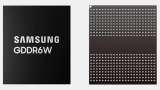
Samsung has introduced its all-new type of GDDR6 memory that doubles the DRAM package's capacity and increases interface width to double its peak bandwidth. Samsung's GDDR6W chips use traditional BGA packaging and can be used for mainstream applications like the best graphics cards.
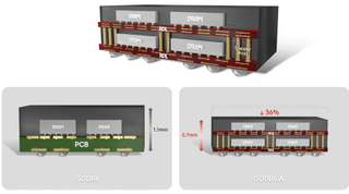
Contemporary GDDR6 and GDDR6X chips integrate one DRAM device with a 32-bit interface. By contrast, a GDDR6W chip packs two DRAM devices featuring and therefore features two 32-bit interfaces, thus doubling capacity (from 16Gb to 32Gb per chip) as well as interface width (from 32-bits to 64 bits). To do so, Samsung's GDDR6W chips use the company's Fan-Out Wafer-Level Packaging (FOWLP) technology that replaces traditional printed circuit board with a redistribution layer (RDL) that is thinner and has significantly finer wiring patterns.

Samsung's GDDR6W devices generally use the same protocols as GDDR6 but offer higher performance and capacity. For example, a 32Gb GDDR6W memory chip could deliver a peak bandwidth of 176 GBps, up from 88 GBps in the case of a regular GDDR6 SGRAM chip. Meanwhile, building a 32Gb memory chip using two 16Gb memory devices might be cheaper than building a 32Gb monolithic memory device.
The memory maker says that usage of FOWLP packaging allows for the reduction of the thickness of GDDR6W packaging to 0.7 mm, down from 1.1 mm in the case of standard GDDR6 chips, making it easier to cool them down. While common sense says that FOWLP packaging is more expensive than traditional BGA packaging, it is unclear how significantly the former is more costly than the latter. Yet, it should be noted that Samsung's GDDR6W should be cheaper than high-bandwidth memory like HBM2E both in terms of memory stack production and usage since GDDR6W does not require the use of expensive interposers.

To put the advertised performance numbers of GDDR6W into context, Samsung says that a 512-bit GDDR6W memory subsystem (which uses eight chips) can provide a system-level bandwidth of up to 1.40 GBps at a 22 GTps data transfer rate. By contrast, a 4096-bit HBM2E memory subsystem offers up to 1.60 TBps at a 3.2 GTps data transfer rate but at a considerably higher price.
Samsung standardized its GDDR6W technology in Q2 2022. After that, the company plans to use its GDDR6W for artificial intelligence, high-performance computing accelerators, and devices like notebooks. Although AMD and Nvidia have yet to support GDDR6W, Samsung says it plans to cooperate with its 'GPU partners' without disclosing the actual companies it works with.
"By applying an advanced packaging technology to GDDR6, GDDR6W delivers twice the memory capacity and performance of similar-sized packages," said CheolMin Park, Vice President of New Business Planning, at Samsung Electronics Memory Business. "With GDDR6W, we are able to foster differentiated memory products that can satisfy various customer needs – a major step towards securing our leadership in the market."
Stay on the Cutting Edge
Join the experts who read Tom's Hardware for the inside track on enthusiast PC tech news — and have for over 25 years. We'll send breaking news and in-depth reviews of CPUs, GPUs, AI, maker hardware and more straight to your inbox.

Anton Shilov is a Freelance News Writer at Tom’s Hardware US. Over the past couple of decades, he has covered everything from CPUs and GPUs to supercomputers and from modern process technologies and latest fab tools to high-tech industry trends.
-
-Fran- Reads cool, but this sounds power hungry and hot right off the bat. I mean, probably worth the trade off vs HBM's implementation, but I would not say HBM is not the better option for true high performance computing as things stand now. Trade offs, for sure.Reply
Sounds interesting, but let's see how it is adopted. I think this will see better adoption on consumer than HPC.
Regards. -
InvalidError Reply
If HBM was mass-manufactured on a scale comparable to GDDR6*, it would likely be cheaper than this fancy double-decked chip-and-PCB sandwich.-Fran- said:Reads cool, but this sounds power hungry and hot right off the bat. I mean, probably worth the trade off vs HBM's implementation, but I would not say HBM is not the better option for true high performance computing as things stand now. Trade offs, for sure. -
thestryker Implementing HBM is pretty much always going to be more expensive due to the interposer. The advantage it has had is density which seems to be what Samsung is primarily aiming at with this technology.Reply -
jp7189 Reply
Likely the production cost of HBM could be cheaper, but I doubt the implementation cost would be. HBM requires a lot of traces.InvalidError said:If HBM was mass-manufactured on a scale comparable to GDDR6*, it would likely be cheaper than this fancy double-decked chip-and-PCB sandwich. -
-Fran- Reply
As others have pointed out, it's not so much the cost of the HBM chip itself, but the whole "close to the CPU/SoC/GPU" restriction and interposer. I do believe you can do it outside of the interposer and use it as GDDR/DDR, but then the traces/routes on the PCB would still make the cost skyrocket compared to GDDR/DDR. The only comparable thing to HBM would be traditional eRAM in both performance and cost (as I understand it).InvalidError said:If HBM was mass-manufactured on a scale comparable to GDDR6*, it would likely be cheaper than this fancy double-decked chip-and-PCB sandwich.
Regards. -
JamesSneed ReplyInvalidError said:If HBM was mass-manufactured on a scale comparable to GDDR6*, it would likely be cheaper than this fancy double-decked chip-and-PCB sandwich.
The interesting thing with this new GDDR6W is it removes the interposer you normally need to do this kind of thing so it's going to be fairly cheap. HBM will never get that cheap unless we hit a point where its used-on package because the 1000's of motherboard traces would be insanely costly. On package it could get cheap enough to see on consumer stuff in a decade or so as it gets used more in HPC then in servers. I could see it making it down the stack in a decade. It would make an awesome APU down on TSMC's 1nm node for example. -
setx While this doubles the density it does pretty much nothing else. From the system point of view, to use 2x capacity and 2x transfer speed you need to have 2x data traces on the board and energy consumption also looks like 2x.Reply
It's a progress but a very weak one. Not comparable to PAM4 on GDDR6X for example. -
InvalidError Reply
The proximity isn't a limitation or restriction until you need more than 128GB and consumer GPUs aren't going to need that much VRAM within the next 20 years. We'll likely have 3D-stacked VRAM within the next 10 years.-Fran- said:As others have pointed out, it's not so much the cost of the HBM chip itself, but the whole "close to the CPU/SoC/GPU" restriction and interposer. -
-Fran- Reply
I'm with you there. I rather GPUs stack HBM and charge me accordingly, but they won't, given the trade offs in cost.InvalidError said:The proximity isn't a limitation or restriction until you need more than 128GB and consumer GPUs aren't going to need that much VRAM within the next 20 years. We'll likely have 3D-stacked VRAM within the next 10 years.
In fact, I'll be surprised AMD goes back to HBM on consumer now that they're doubling down on stacked cache. I can absolutely see VCache+HBM on datacenter and HPC (in particular), but not in consumer space; sadge.
Regards.
Most Popular


