Stanford Researchers Leverage Palladium for Disruptive Memristor Design

Palladium periodic table
(Image credit: Shutterstock)

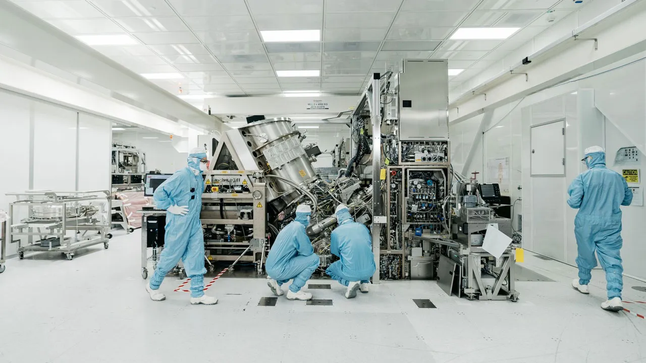
Let's face it: While Moore's Law may not be completely dead, it's been on life support for a while. Long gone are the days of "easy" performance uplifts from improving manufacturing processes and simple transistor size reduction. These days, R&D teams looking to improve semiconductor performance year upon year have to branch out into not only the transistor architecture itself, but also into materials engineering. Exploring elements present in the periodic table might give semiconductors a more performant, smaller, and energy-efficient design than silicon can provide. Now, a research team with the School of Engineering at Stanford has turned to one of the most precious metals on Earth - palladium - as a potential venue for faster, cooler, and more energy-efficient memory architectures.

The research team's approach is based on the assumption that we've transitioned from the Internet era and are already knee-deep in the AI era. According to Shan Wang, the Leland T. Edwards Professor in the School of Engineering at Stanford University, the idea behind the research was to "enable AI on edge – training locally on your home computer, phone, or smartwatch – for things like heart attack detection or speech recognition." 

Yet to do that, he added, our current technological crop won't cut it; we need a type of memory that's been on again, off again in the press without a single product being brought to market: memristors. Memristors are a type of non-volatile memory that doesn't require a constant stream of electricity to keep data in its memory banks (check here for a more detailed breakdown of memristor tech). The first author of the paper, Mahendra DC, explained it best: “We are hitting a wall with the current technology,” DC says. “So we have to figure out what other options we have.”

To break that wall, the researchers singled out a compound of palladium, manganese palladium three, as having the necessary properties to finally (they say) enable a memristor design to see the light of day. Part of the checklist pertains to our current semiconductor manufacturing tech: any material being considered for novel semiconductor designs has to deal with the fact that tooling and supply lines are entrenched in the silicon realm. So any alternative compound will ideally be able to be slotted into current manufacturing processes without the need for extensive (and expensive) process changes.

Manganese palladium three fits that bill, yet the most important property of the compound is the way in which its particles are manipulated to become memory storage devices. Information here is derived not from a voltage state, as is the case with standard memory devices such as NAND flash, but by manipulating the spin orientation of the compound's electrons. Essentially, researchers are able to manipulate an electron's magnetic field, bouncing its center between the north and south poles. Then one of these spin directions (north-south or south-north) is made to represent a 1 or a 0 - unlocking the binary system behind computing as we know it. Named "spin orbit torque magnetoresistive random access memory", or SOT-MRAM for a necessary shortening, this spin data storage method has the potential to store data faster and more efficiently than current technology allows - and at higher densities as well.

Of course, there's one big caveat in all this research: Palladium is currently almost as expensive as gold, but is also a much rarer commodity. To make matters worse, 40% of the world's palladium is currently mined in South Africa, with 44% more being mined in Russia. So palladium availability might itself be a problem from the logistics and geopolitics side of the equation. Beyond that, increased demand for palladium for SOT-MRAM would certainly drive its price up even higher. All off this will need to be considered when pursuing novel transistor designs.

All in all, the research is promising, but like all memristor news in the last decade (and longer), it seems that we're still standing at the beginning of the proverbial yellow brick road. Whether or when we see the castle at the end, well, that's for the future to tell us.

Francisco Pires
Freelance News Writer

Francisco Pires is a freelance news writer for Tom's Hardware with a soft side for quantum computing.

  • Metal Messiah.
    Well, it's good to know they are suing Palladium fro Memristors, but I doubt the availability and the widespread usage pf this compound. The amounts of palladium like gold isn't that commonly used in electronics.

    Current alternative SOT-MRAM contenders (excluding optane). Most are phased out now, but I was hoping Nantero will do more breakthroughs in Nano-RAM tech, but they haven't:
    Ferroeletric RAM (FeRAM)
    Magnetoresistive RAM (MRAM)
    Phase-change memory (PCM)
    Resistive RAM (ReRAM)
    Nano-RAM (NRAM)But assuming if SOT-MRAM becomes the next mainstream MEM technology, they can try and find a better material as switchover to it, but nonetheless, the cost of palladium would not overall be a major roadblock for this technology.

    But since we're talking micrograms of palladium per chip vs milligrams of gold, the amount is minimal, and unless I'm mistaken, thickness of the MnPd layer is just 10nm, so based on this, for a 100mm2 chip a single layer would have ~8μg of it, costing ~0.04 cents at current price. In future who knows the availability/cost of palladium though. :rolleyes:

    But there are other problems first need to be taken care of apart form the cost of palladium.
    Reply
  • Metal Messiah.
    Btw, I found this technical paper which is also worth giving a read:

    https://arxiv.org/ftp/arxiv/papers/2012/2012.09315.pdf
    Reply
  • kjfatl
    We all know that there are 4 fundamental 2-terminal circuit elements:
    Resistor, Capacitor, Inductor and Memristor.
    In circuits class, some of us were sleeping the day memristors were introduced.
    A 6-minute memristor guide is shown below for those who missed this material.
    rvA5r4LtVncView: https://www.youtube.com/watch?v=rvA5r4LtVnc
    Reply
  • usertests
    Metal Messiah. said:
    But since we're talking micrograms of palladium per chip vs milligrams of gold, the amount is minimal, and unless I'm mistaken, thickness of the MnPd layer is just 10nm, so based on this, for a 100mm2 chip a single layer would have ~8μg of it, costing ~0.04 cents at current price. In future who knows the availability/cost of palladium though. :rolleyes:

    But there are other problems first need to be taken care of apart form the cost of palladium.
    Sounds like the palladium isn't really a problem at all and the semiconductor industry demand would pale in comparison to the amount of palladium used in automotive catalytic converters. If trillions of SoCs are being produced with palladium memristors 20 years from now, they can mine more from asteroids.
    Reply
  • kjfatl
    The biggest use of palladium is catalytic converters for gasoline engines.
    With the push toward EV's will this cause the price of palladium to drop?
    Reply
  • Metal Messiah.
    I think you guys are correct. Let's see what the future holds for palladium. Btw, that's a pretty old video on memristors which I think I have watched before. Thanks for the brush up.

    Also yes, Palladium is used in a wide range of applications, from dentistry to fertilizer manufacturing, but by far the most important application is as an active component in catalytic converters in the automotive field like you mentioned.

    Most of palladium is used for exhaust treatment of gasoline vehicles. I heard they are trying to replace palladium with platinum/Pt in gasoline vehicle catalysts in near future.
    Reply
  • Metal Messiah.
    This one is actually a pretty good and informative lecture/video if anyone wants to learn more about Memristors, or just brush up the basics. Worth watching:

    Z5UTRTOfgo4View: https://www.youtube.com/watch?v=Z5UTRTOfgo4&ab_channel=CITRIS
    Reply
  • Metal Messiah.
    BTW, a very informative article I just stumbled upon.

    In the future, memristor appears to be a promising candidate for high-density, high-energy efficiency, ultra-fast, low-latency, low power, large-capacity non-volatile memory. Therefore, many companies (Samsung, Panasonic, HP, Micron, Sony, Yangtze Memory Technologies Co., Ltd. (YMTC), Crossbar etc.) are engaged in research and development of memristors.

    These memristor arrays can build more integrated neural network structures, including artificial neural networks (ANN) convolutional neural networks (CNNs), deep neural networks (DNNs), recurrent neural networks (RNNs), and spike neural networks (SNNs).

    The second article which is actually referencing an old thesis, however focuses on design strategies, performance superiorities, and technical drawbacks of various memristors in relation to ANN applications, as well as the updated versions of ANN, such as deep neutral networks (DNNs) and spike neural networks (SNNs).

    So to extend the limits of Moore’s law, memristors, whose electrical and optical behaviors closely match the biological response of the human brain, have been implemented for ANNs in place of the traditional complementary metal-oxide-semiconductor (CMOS) components.

    https://www.ncbi.nlm.nih.gov/pmc/articles/PMC9980037/
    https://www.frontiersin.org/articles/10.3389/fphy.2022.839243/full
    Reply