A blogger has published estimates of TSMC’s wafer costs and prices. Quite unsurprisingly, processing of wafers is getting more expensive with each new manufacturing technology as nodes tend to get more capital intensive. TSMC’s latest N5 (5nm) fabrication process appears to be particularly expensive on per-wafer basis because it is new, but its transistor density makes it particularly good for chips with a high transistor count.
RetiredEngineer, a well-known semiconductor blogger, has published a table with a calculation of TSMC’s sale price per hypothetical chip by node in 2020. The source of the table was not mentioned, but it probably comes from a recent report covering foundry business and makers of semiconductors.
The model is based on an imaginary 5nm chip the size of Nvidia's P100 GPU (610 mm2, 90.7 billion transistors at 148.2 MTr/mm2). As far as foundry sale price per patterned 300-mm wafer is concerned, the model takes into account such things as CapEx, energy use, depreciation, assembly, test and packaging costs, foundry operating margins, and some other factors. Meanwhile, the foundry sale price per chip also includes design costs, yet this number varies greatly from company to company and from node to node (i.e., design costs of a 610 mm2 5nm are different for different companies and implementation of a 610 mm2 chip varies from node to node due to different design rules and IP), so it should be taken with a grain of salt.

According to the estimates, TSMC sells a 300mm wafer processed using its N5 technology for about $16,988. By contrast, the world’s largest contract maker of semiconductors charges around $9,346 per 300mm wafer patterned using its N7 node as well as $3,984 for a 300mm wafer fabbed using its 16nm or 12nm technology.
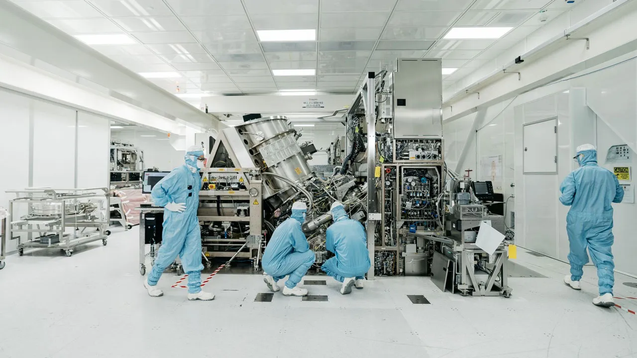
There are several factors that make TSMC’s N5 node so expensive to use today. Firstly, TSMC started to produce 5nm chips several months ago and the fab as well as equipment it uses have not depreciated yet. Secondly, N5 heavily relies on usage of extreme ultraviolet lithography and can use it on up to 14 layers. According to ASML, one EUV layer requires one Twinscan NXE step-and-scan system for every ~45,000 wafer starts per month. Each EUV tool is believed to cost about $120 million and these scanners are rather expensive to run, too. Given TSMC’s volumes, it needs loads of such scanners for its N5 technology. Therefore, it will take some time before TSMC depreciates the fab and equipment it uses for N5.

But even at current costs it makes a great sense for makers of highly-complex chips to use TSMC’s leading-edge process because of its high transistor density as well as performance. Based on the numbers provided, it costs $238 to make a 610mm2 chip using N5 and $233 to produce the same chip using N7. At 16/12nm node the same processor will be considerably larger and will cost $331 to manufacture. At N5, the chip will not only be relatively small (at 610mm2 to be more precise), but it will also run 15% faster at a given power or consume 30% less power at a given frequency when compared to N7.

According to TSMC, its N5 has a lower defect density than N7 at the same time of its lifespan, so chip designers can expect that eventually N5-based chips will yield better than N7-based ICs in general. The latter is something to expect given the fact that N5 replaces DUV multi-patterning with EUV single patterning.
One thing to keep in mind with such a comparison between nodes is that while it is based on data from TSMC as well as the semiconductor industry in general, the actual numbers have never been confirmed by the Taiwanese giant, so they may not be a 100% accurate.