







Intel surpasses one million High-NA EUV wafers processed, outpaces the rest of the industry combined — company also trailblazing giant 6×12 photomasks to speed production and lower costs
Stitching to be used in the near term future with High-NA tools, but larger 6×12 photomasks envisioned.

Intel announced on Monday that it had processed more than one million 300-mm wafers using its High-NA EUV scanners, less than two and a half years after its first tool was assembled. For now, the company intends to use industry-standard 6-inch photomasks, which can expose 26×16.5 mm half-fields and therefore require field stitching for larger chips. However, Intel is also working on larger 6×12-inch photomasks that would enable High-NA EUV scanners to expose full 26×33 mm fields without stitching.
One million High-NA wafers
Intel's one million wafers figure includes wafers processed during tool installation and certification, R&D, and production. Earlier this year, Intel certified using High-NA EUV scanners for its 18A process technology, so right now these tools are used to make some of Intel's Panther Lake processors. Intel currently has two ASML Twinscan EXE:5000 tools and at least one EXE:5200B scanner. As of late February 2025, Intel processes around 30,000 wafers using its High-NA EUV tool, so going from 30,000 wafers by February 2025 to over a million by September 2026 is an enormous increase in cumulative High-NA utilization.
Since Intel's fleet expanded from two EXE:5000 systems to three and now includes the much faster EXE:5200B, the million-wafer milestone is really a fleet and process-maturity milestone that Intel has achieved first in the industry. What makes the company's milestone even more important is that ASML announced this April that all of the High-NA EUV scanners shipped by then processed over 500,000 wafers which achieving over 80% availability, which means that Intel has now processed more wafers using High-NA tools than the rest of the industry combined.
Sticking to stitching
Conventional 0.33-NA EUV has 4X magnification in both directions, enabling the familiar 26×33 mm exposure field with traditional 6-inch photomasks. However, 0.55-NA EUV uses anamorphic 4X/8X magnification, so the same 6×6 mask can provide only approximately 26×16.5 mm on the wafer. As a result, large dies that fit within a conventional 26 × 33 mm EUV field must be exposed as two half-fields using High-NA EUV, which is called stitching. While stitching is a workable near-term solution, it has several drawbacks.
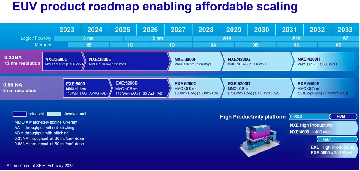
Firstly, it greatly reduces throughput from 175 wafers per hour to 125 wafers per hour on an EXE:5200B. Secondly, chip designs must account for stitching and must be developed with stitching in mind, which means less floor planning freedom. Thirdly, the two exposures must be aligned extremely precisely so that features crossing the stitching boundary connect properly. Even a tiny misalignment can distort lines and vias, or break interconnects, which potentially creates defects and reduces yields, which will be a particularly costly problem for large CPU and GPU dies.
6×12 mask effort progressing
To avoid using stitching, the industry — led by Intel — plans to shift to larger 6×12 masks, which will enable a 26×33 mm full field in one exposure. While this looks easy on paper, make the mask twice as long, changing the mask represents an enormous ecosystem change.
Get Tom's Hardware's best news and in-depth reviews, straight to your inbox.
Moving from 6×6-inch to 6×12-inch photomasks would require substantial changes across the existing mask ecosystem, including mask blanks and deposition, etching, inspection and metrology, cleaning, pellicles, mask writers, and mask handling systems. Crucially, High-NA EUV scanners would also have to be modified or redesigned to accommodate the larger masks, which will make the transition a major retooling effort across the semiconductor supply chain. While neither ASML nor Intel confirmed that existing or planned High-NA EUV scanners can be modified to handle larger masks, all of the future High-NA EUV scanners to be launched before and after 2033 are designed around 6×6-inch reticles and stitching, according to ASML's roadmap.
It remains to be seen whether the industry moves on to larger 6×12-inch photomasks, but Intel appears to be the main evangelist for changing the mask standard that has defined projection lithography infrastructure for decades. If the effort comes to fruition, then Intel will likely have a considerable first-mover advantage over its industry peers because it will define and set the standard for the projection lithography industry for decades to come, an advantage that is hard to overestimate.

Follow Tom's Hardware on Google News, or add us as a preferred source, to get our latest news, analysis, & reviews in your feeds.

Anton Shilov is a contributing writer at Tom’s Hardware. Over the past couple of decades, he has covered everything from CPUs and GPUs to supercomputers and from modern process technologies and latest fab tools to high-tech industry trends.
-
mac2213 The reporting on the technical details in this article is outstanding, but it fails to recognize the confusing information that both Intel and ASML had pushed on the market regarding HNA tool deliveries starting in the spring of 2024. Even the recent comments by ASML at Semicon Taiwan 26 were intentionally misleading, but a bit closer to the truth where they talked about 4 HNA customers and 13 total HNA tools delivered, but failed to include IMEC and NY Crest Dev efforts in either count. It would be nice if Tom's could lead the reporting on the tool count and timing on delivery in their reporting. Restating the belief that Intel only has 3 or 4 tools out of 13 total (or 16 including IMEC/NYDEV) doing this kind of volume is confusing everyone further.Reply -
moreslawplease Reply
Intel could have easily made a million wafers in this time with just one machine. Check ASML page for the 5000. Output is still 100+ per hour. It's not like they are claiming 1M fully finished wafers using every feature of high na... I'm not saying it's one but the million doesn't mean it needs to be more than one either.mac2213 said:The reporting on the technical details in this article is outstanding, but it fails to recognize the confusing information that both Intel and ASML had pushed on the market regarding HNA tool deliveries starting in the spring of 2024. Even the recent comments by ASML at Semicon Taiwan 26 were intentionally misleading, but a bit closer to the truth where they talked about 4 HNA customers and 13 total HNA tools delivered, but failed to include IMEC and NY Crest Dev efforts in either count. It would be nice if Tom's could lead the reporting on the tool count and timing on delivery in their reporting. Restating the belief that Intel only has 3 or 4 tools out of 13 total (or 16 including IMEC/NYDEV) doing this kind of volume is confusing everyone further. -
adamXpeter So TMSC multi-pass to avoid buying these machines and Intel multi-pass because they bought these machines?Reply -
mac2213 Reply
Without sharing all that I know here, I'm pretty sure my data would convince you that you are wrong. I would share privately with you if that is possible and you are interested.moreslawplease said:Intel could have easily made a million wafers in this time with just one machine. Check ASML page for the 5000. Output is still 100+ per hour. It's not like they are claiming 1M fully finished wafers using every feature of high na... I'm not saying it's one but the million doesn't mean it needs to be more than one either. -
EzzyB ReplyIf the effort comes to fruition, then Intel will likely have a considerable first-mover advantage over its industry peers because it will define and set the standard for the projection lithography industry for decades to come, an advantage that is hard to overestimate.
Intel payed a premium to get the first of these machines some time ago when they were mired in their 12 and 10nm (class) then used TSMC to bridge the gap. And, they did it at a time when many were declaring Intel's imminent demise. It's looking like it may very well be paying off for them.
I remember saying at the time that Intel hadn't forgotten how to make computer chips. I know very few of the commentariat here like to hear anything at all positive about Intel, but, good things like this simply drive on the fierce competition that keeps our processors getting better and better. Will AMD/TSMC respond? Of course they will in time and that's good for all of us.
I'd love to see Intel use this technology to build a 5070/5070ti class Arc GPU priced around $450. It would set the GPU market on it's head and force more competition there. Almost certainly a pipe dream, but a good one. -
Eximo ReplyEzzyB said:I'd love to see Intel use this technology to build a 5070/5070ti class Arc GPU priced around $450. It would set the GPU market on it's head and force more competition there. Almost certainly a pipe dream, but a good one.
My understanding is they shuttered every project below a certain profitability. Bringing their GPU production under their roof would only help a little, the rest of the build costs are still there, and still inflated. Memory, PCB fab, assembly, etc all outsourced.
A more realistic hope is that Nvidia (possibly AMD as well) moves their mid-range GPUs to Intel fabs. Intel could use a steady customer or two, and it would save more of the top-spec TSMC fab time for the stuff they clearly deem more important. -
usertests Reply
Based on the article, they are using it for Panther Lake, but not from the beginning. Panther Lake is generally recognized as a good APU, albeit expensive in these trying times.Stomx said:1 Million, 1 Billion...Where is something I'd like to buy ? -
EzzyB Replyusertests said:Based on the article, they are using it for Panther Lake, but not from the beginning. Panther Lake is generally recognized as a good APU, albeit expensive in these trying times.
My thoughts were a bit darker. Many, many companies in AI are now designing their own chips for fabrication somewhere. Microsoft, Meta, Google, Open AI, and Anthropic I believe are all doing it. So any open capacity is going to get snapped up for things like that.Eximo said:My understanding is they shuttered every project below a certain profitability. Bringing their GPU production under their roof would only help a little, the rest of the build costs are still there, and still inflated. Memory, PCB fab, assembly, etc all outsourced.
A more realistic hope is that Nvidia (possibly AMD as well) moves their mid-range GPUs to Intel fabs. Intel could use a steady customer or two, and it would save more of the top-spec TSMC fab time for the stuff they clearly deem more important.
There was some talk only a few months ago that Intel was working with Apple to fab it's M processors as well.