TSMC details 12.8 Tbps on-package optical communications — an efficient silicon photonics interconnect for AI
TSMC announces COUPE optical photonics platform.

Rumors about TSMC having a silicon photonics program have been around for a long time, and at its Northern American Technology Symposium 2024, the company finally outlined its solution. The goal is to improve on-package connectivity, spanning all the way to 12.8 Tbps of bandwidth.
"As we bring more computational capability into the mass packaging, data transfers become a challenge, but we find ourselves often limited by the I/O vendors," said Kevin Zhang, Vice President of Business Development at TSMC. "At TSMC, we have spent many, many years working on silicon photonics. We have the capability to bring silicon photonics close to the switching elements in order to create a very energy efficient high-speed signaling to address the future computation requirement."
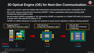
Silicon photonics is set to be a game-changer for future datacenters due to increasing bandwidth demands that copper signaling just cannot meet. TSMC's silicon photonics technology relies on the Compact Universal Photonic Engine (COUPE) that combines a 65nm electronic integrated circuit (EIC) with a photonic integrated circuit (PIC) using the company's SoIC-X packaging technology. TSMC claims that its SoIC-X interconnection has very low impedance, which means that COUPE is very efficient in terms of power usage.

The development trajectory of COUPE has three major phases. TSMC's first silicon photonics product is an optical engine for OSFP connectors (Octal Small Form Factor Pluggable) that features a data transfer rate of 1.6 Tbps, twice the maximum of current top-tier copper Ethernet solutions. This initial iteration promises not just superior bandwidth but also improved power efficiency, addressing two critical concerns in modern datacenters. Subsequent generations of COUPE aim to push the boundaries further.
The second generation silicon photonics will integrate COUPE into CoWoS packaging (Chip on Wafer on Silicon) and features co-packaged optics with a switch. This will enable motherboard-level optical interconnections with speeds of up to 6.4 Tbps.
The third generation targets transfer rates of up to 12.8 Tbps and is designed to be integrated into processor packaging. This iteration is still in the exploratory phase, with no definite release timeframe. TSMC says it's looking at further reductions in power use and latency.
TSMC's strategic pivot into the silicon photonics market, previously dominated by companies like GlobalFoundries, indicates a significant shift in the competitive landscape. By deploying its 3D Optical Engine, TSMC not only enters a crucial datacenter connectivity field, but it plans to significantly reduce power consumption of silicon photonics technology. This could significantly impact future chip designs, particularly in the area of AI workloads where communication is becoming a significant bottleneck.
Stay On the Cutting Edge: Get the Tom's Hardware Newsletter
Get Tom's Hardware's best news and in-depth reviews, straight to your inbox.

Anton Shilov is a Freelance News Writer at Tom’s Hardware US. Over the past couple of decades, he has covered everything from CPUs and GPUs to supercomputers and from modern process technologies and latest fab tools to high-tech industry trends.
-
Diogene7 I am wondering if the integration of this silicon photonics technology could help create an Apple Pro Display XDR, that would have the same kind of connector used to connect to the Apple Pro stand (the magnetic circle) but that would also integrate silicon photonics connectivity : this would allow relocating the I/O to the bottom of the stand, and have integrated optical fibers inside the stand to transfer data from I/O (Thunderbolt 4, HDMI,…) to the display…Reply -
HaninTH Reply
More likely, 20+ years as the industry has been talking about SiPho for at least 20 years with Intel showing some early progress 10+ years ago.Lucky_SLS said:Aimed at data center, might trickle down to mainstream products in 10 years?
Will be interesting to see this technology realized. -
Lucky_SLS ReplyHaninTH said:More likely, 20+ years as the industry has been talking about SiPho for at least 20 years with Intel showing some early progress 10+ years ago.
Will be interesting to see this technology realized.
In this case, the adaption would be quicker as TSMC is releasing the tech for its customers. Its not locked to Intel. So chip designers would readily adapt them if the price and performance proves beneficial. -
bit_user Reply
Right now, I can't even see a use case for this in consumer machines. That doesn't mean it won't happen within 10 years, but I just can't see far enough ahead to have an idea of what sorts of problems would justify it.Lucky_SLS said:In this case, the adaption would be quicker as TSMC is releasing the tech for its customers. Its not locked to Intel. So chip designers would readily adapt them if the price and cost proves beneficial. -
Lucky_SLS Replybit_user said:Right now, I can't even see a use case for this in consumer machines. That doesn't mean it won't happen within 10 years, but I just can't see far enough ahead to have an idea of what sorts of problems would justify it.
Apple: challenge accepted XD
Most Popular


