China's First Wafer Regeneration Facility Enters Mass Production
Reducing the amount of wasted silicon from semiconductor manufacturing.

Get Tom's Hardware's best news and in-depth reviews, straight to your inbox.
You are now subscribed
Your newsletter sign-up was successful
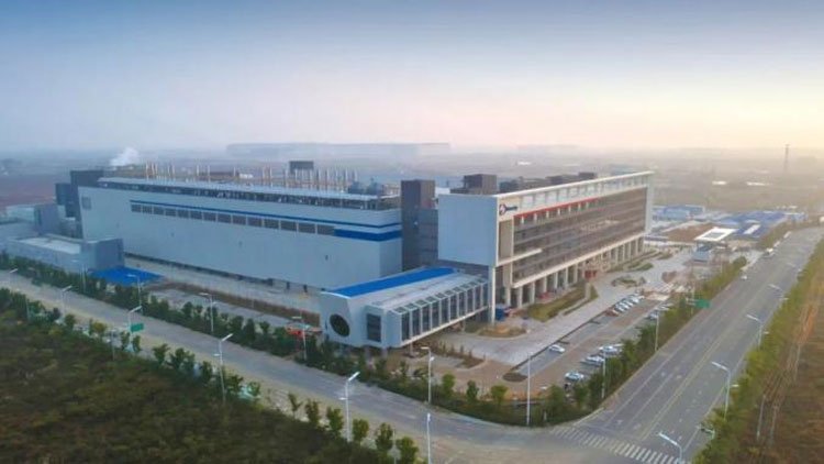
Chinese company Hefei Ultron Semiconductor Co has announced that it has achieved mass production on its silicon wafer regeneration facilities in the eastern province of Hanui. This marks the first such facility operating in China, enabling local semiconductor manufacturers to recover damaged or contaminated 12-inch wafers within the country's borders. As reported by CnTechPost.
As is the case with any manufacturing process, semiconductor manufacturing does have deviations from the established "perfect" production scenarios. Even in semiconductor fabrication facilities, some of the world's most tightly-controlled environments, there is still room to fail - whether in the wafer etching process that extract chips out of the prime silicon matter, or by using contaminated prime materials for the various manufacturing steps. Errors are costly here, and while some imperfections result in a reduction in yield (the percentage of useable, conforming silicon at the end of fabrication), other errors - such as contamination or power outages - can throw companies back thousands of dollars, undoing months of careful fabrication steps for a single silicon wafer.
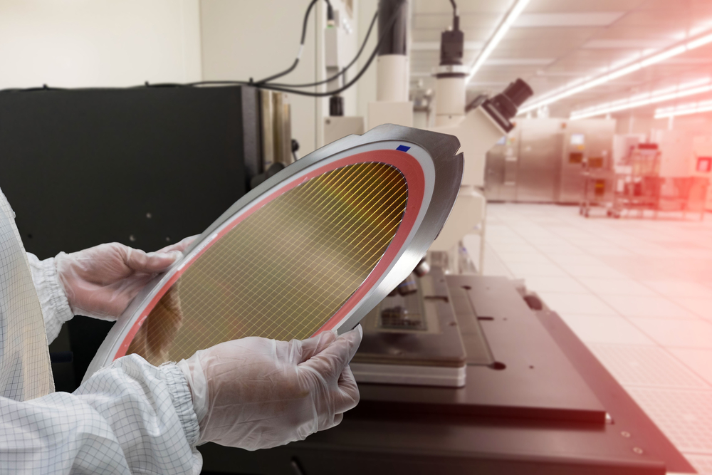
Wafer regeneration is a catch-all term, referring to the processes that transforms contaminated and/or impurity-laden wafers back into their pristine, original condition - ready for another go-around in the fabrication rooms. The process can present itself in different ways: one such process can be done in a three-step pipeline, where diamond abrasive disks are used to grind away the etched layers and eliminate structures from the wafer; a second pass chemically polishes the wafer surface back to pristine condition; and a final step chemically cleans the entire wafer surface. The regenerated wafers are then packed and sent back to the client, who can then insert them back into their fabrication pipeline.
The wafer regeneration facility from Hefei Ultron Semiconductor Co now joins a limited number of such facilities around the world, and will provide Chinese semiconductor manufacturers with an in-border partner - previously, unusable wafers had to be sent to be Japan to receive the same treatment.

Construction of the factory started in March 2020, and the total investment totalled around $154 million. Hefei Ultron Semiconductor Co expects the facility to regenerate 1.68 million wafers per years, with additional capacity installed to clean other manufacturing parts at a rate of 1.2 million per year.
Get Tom's Hardware's best news and in-depth reviews, straight to your inbox.

Francisco Pires is a freelance news writer for Tom's Hardware with a soft side for quantum computing.