TSMC mulls massive 1000W-class multi-chiplet processors with 40X the performance of standard models
A 9.5x reticle size SiP on a massive substrate.
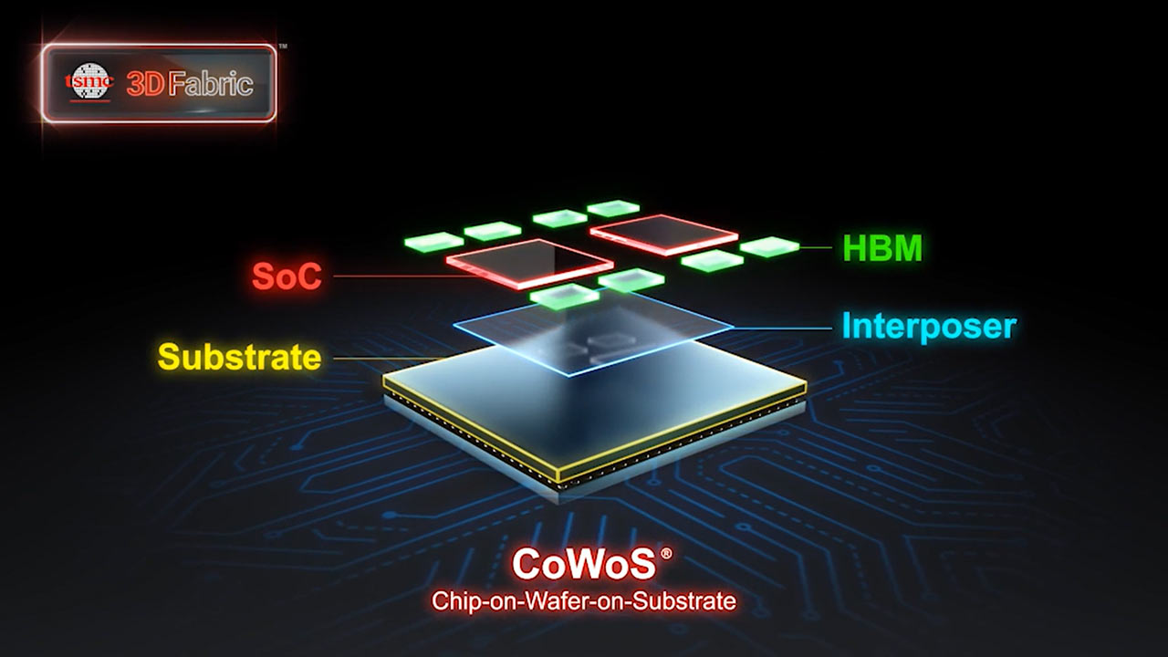
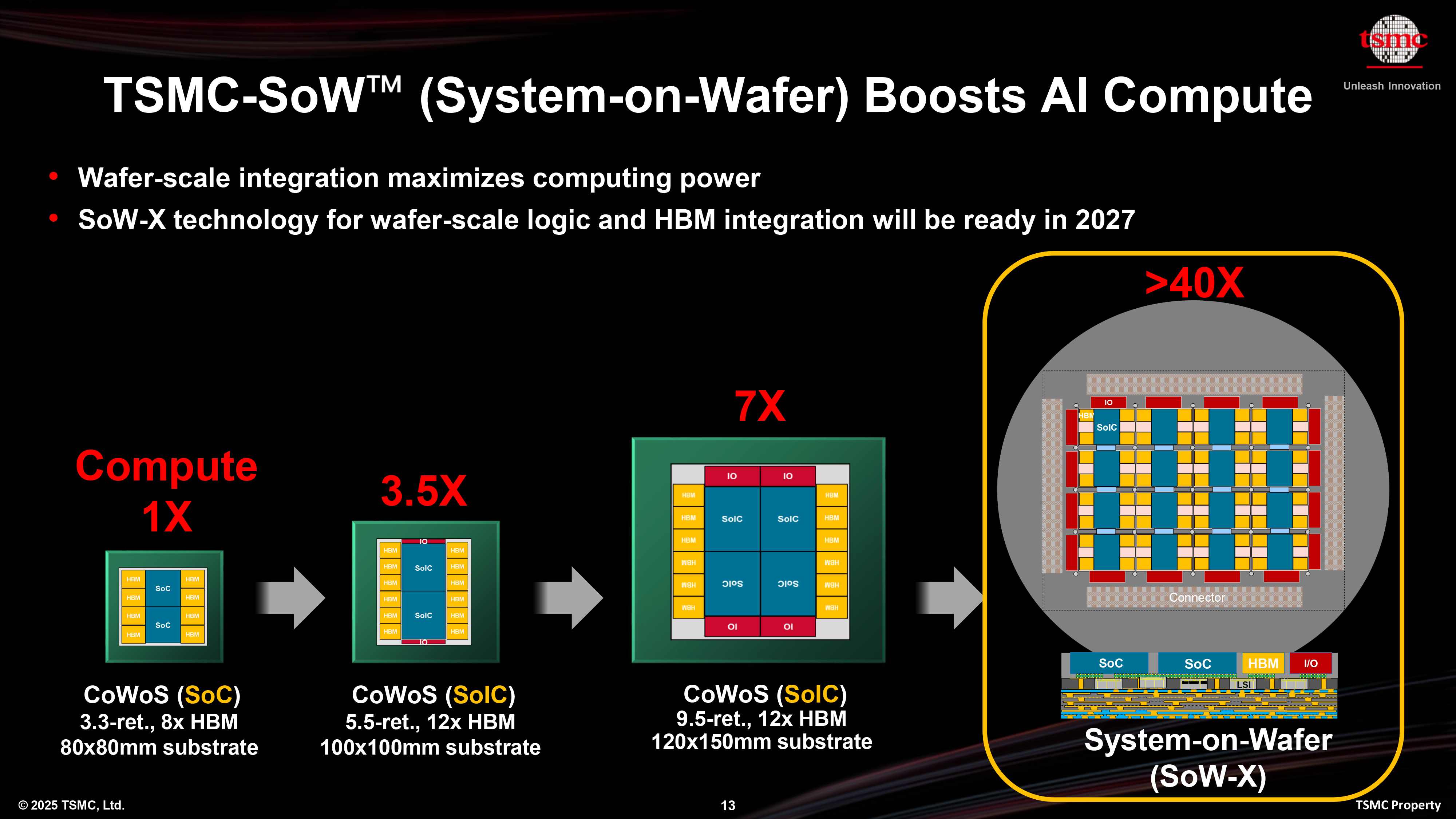
You might often think of processors as being relatively small, but TSMC is developing a version of its CoWoS technology that will enable its partners to build multi-chiplet assemblies that will be 9.5-reticle sized (7,885 mm^2) and will rely on 120×150 mm substrates (18,000 mm^2), which is slightly larger than the size of a CD case. TSMC claims these behemoths could offer up to 40 times the performance of a standard processor.
Virtually all modern high-performance data center-grade processors use multi-chiplet designs, and as demands for performance increase, developers want to integrate even more silicon into their products.
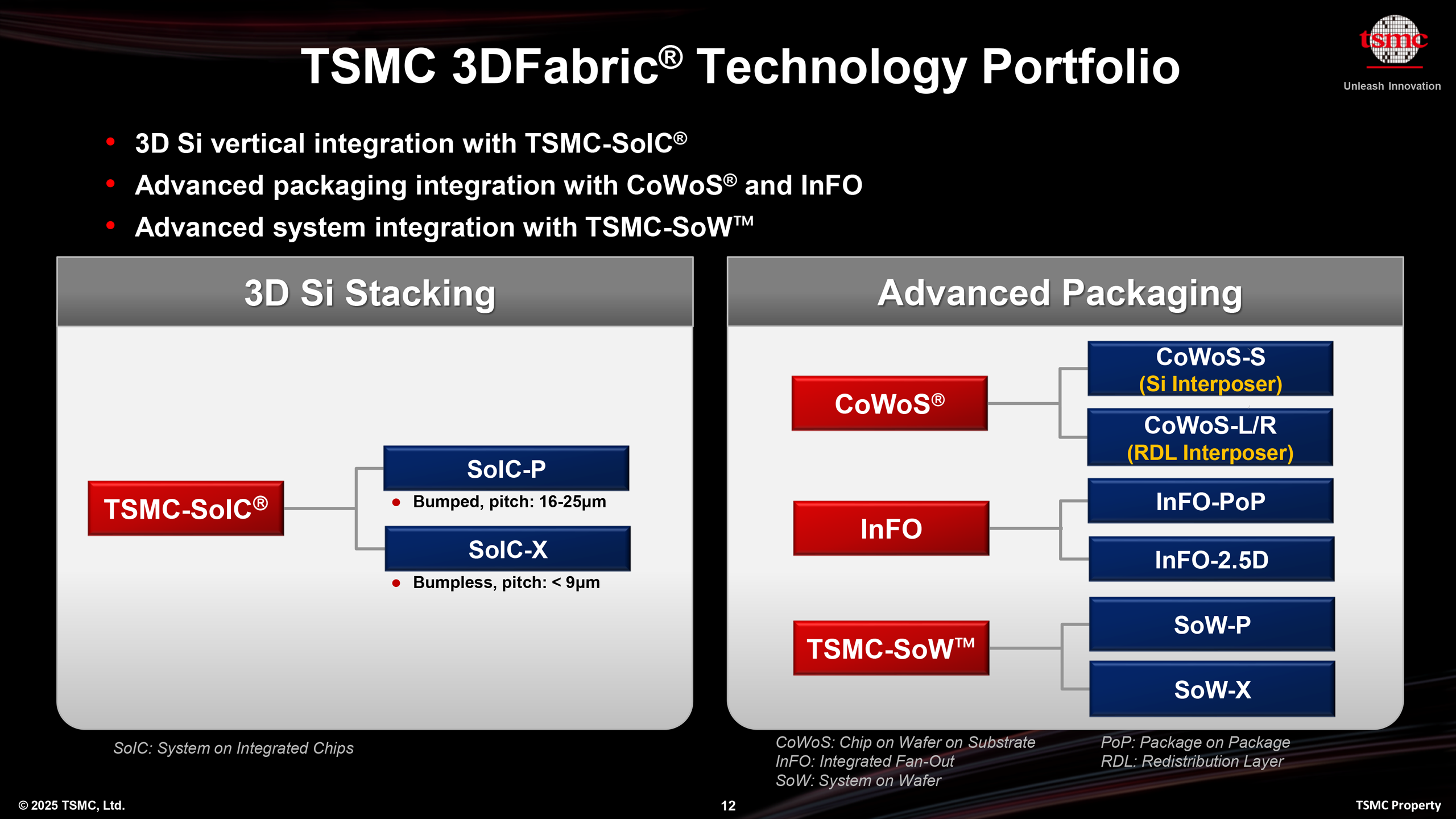
In an effort to meet demand, TSMC is enhancing its packaging capabilities to support significantly larger chip assemblies for high-performance computing and AI applications. At its North American Technology Symposium, TSMC unveiled its new 3DFabric roadmap, which aims to scale interposer sizes well beyond current limits.
From big to huge
Currently, TSMC CoWoS offers chip packaging solutions that enable interposer sizes of up to 2831 mm^2, which is approximately 3.3 times larger than the company’s reticle (photomask) size limit (858 mm^2 per EUV standard, with TSMC using 830 mm^2). This capacity is already utilized by products like AMD’s Instinct MI300X accelerators and Nvidia’s B200 GPUs, which combine two large logic chiplets for compute with eight stacks of HBM3 or HBM3E memory. But that's not enough for future applications.
Sometimes next year, or a bit later, TSMC plans to introduce the next generation of its CoWoS-L packaging technology, which will support interposers measuring up to 4,719 mm^2, roughly 5.5 times larger than the standard reticle area. The package will accommodate up to 12 stacks of high-bandwidth memory and will require a larger substrate measuring 100×100 mm (10,000 mm^2). The company expects that solutions built on this generation of packaging will deliver more than three and a half times the compute performance of current designs. While this solution may be enough for Nvidia’s Rubin GPUs with 12 HBM4 stacks, processors that will offer more compute horsepower will require even more silicon.
Looking further ahead, TSMC intends to scale this packaging approach even more aggressively. The company plans to offer interposers with an area of up to 7,885 mm^2, approximately 9.5 times the photomask limit, mounted on a 120×150 mm substrate (for context, a standard CD jewel case measures approximately 142×125 mm).
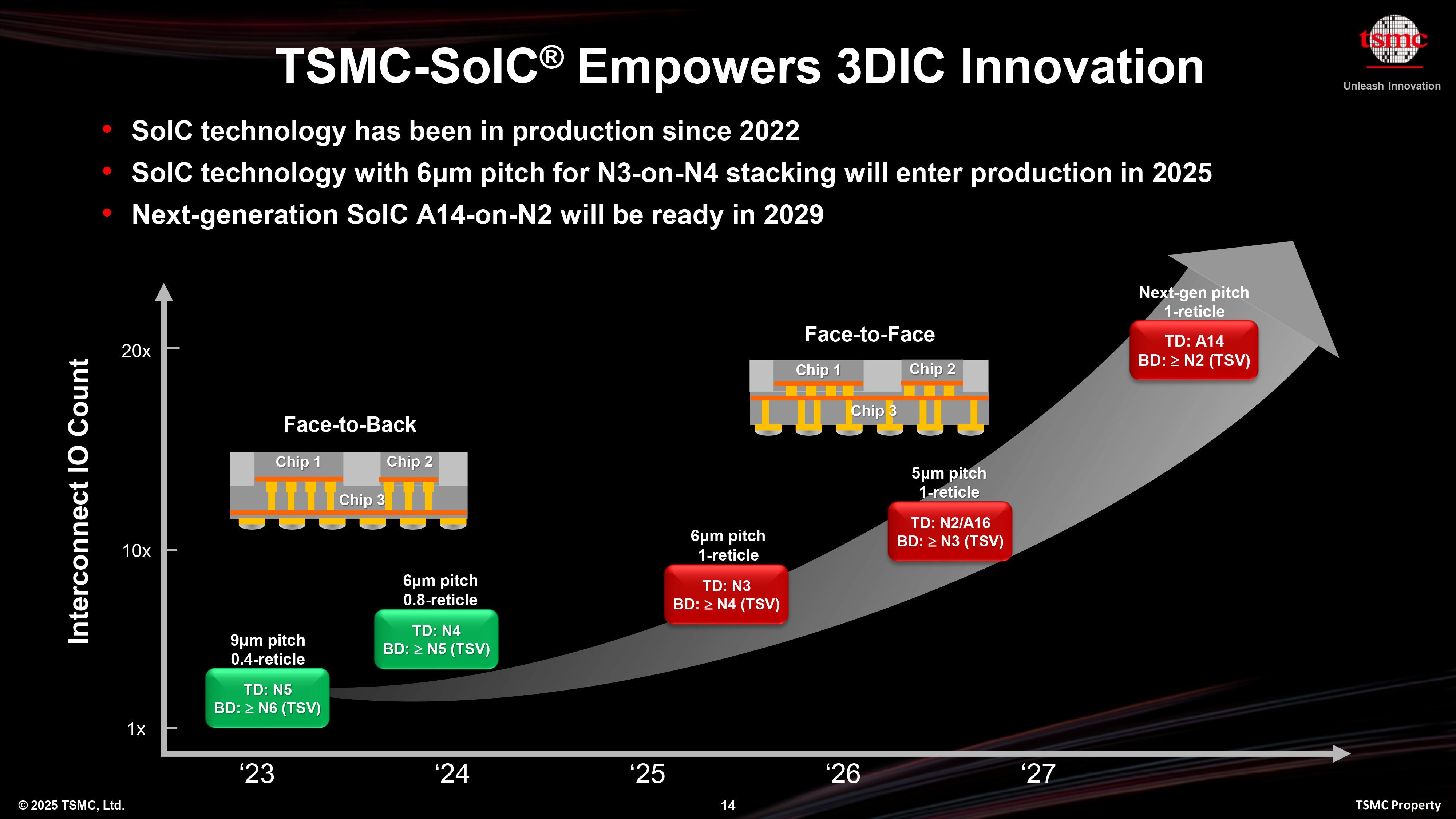
This represents an increase from an 8x-reticle-sized multi-chiplet assembly on a 120×120mm substrate that TSMC presented last year, and this increase likely reflects the requests from the foundry's customers. Such a package is expected to support four 3D stacked systems-on-integrated chips (SoICs, e.g., an N2/A16 die stacked on top of an N3 logic die), twelve HBM4 memory stacks, and additional input/output dies (I/O Die).
However, TSMC has customers who demand extreme performance and are willing to pay for it. For them, TSMC offers its System-on-Wafer (SoW-X) technology, which enables wafer-level integration. For now, only Cerebras and Tesla use wafer-level integration for their WFE and Dojo processors for AI, but TSMC believes there will be customers beyond these two companies with similar requirements.
Get Tom's Hardware's best news and in-depth reviews, straight to your inbox.
Power delivery
Without a doubt, 9.5-reticle-sized or wafer-sized processors are hard to build and assemble. But these multi-chiplet solutions require high-current kilowatt-level power delivery, and this is getting harder for server makers and chip developers, so it needs to be addressed at the system level. At its 2025 Technology Symposium, TSMC outlined a power delivery strategy designed to enable efficient and scalable power delivery at kilowatt-class levels.
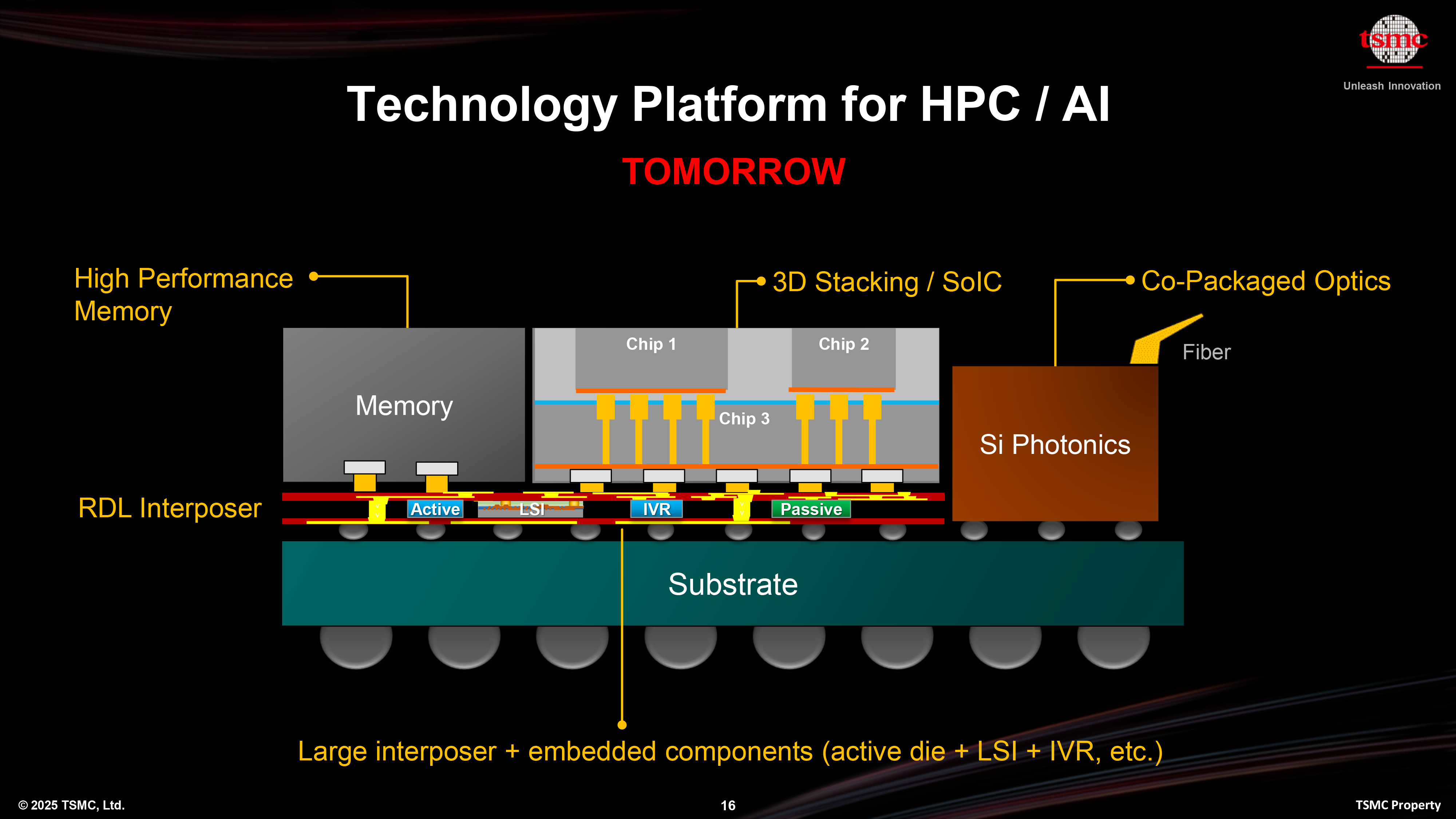
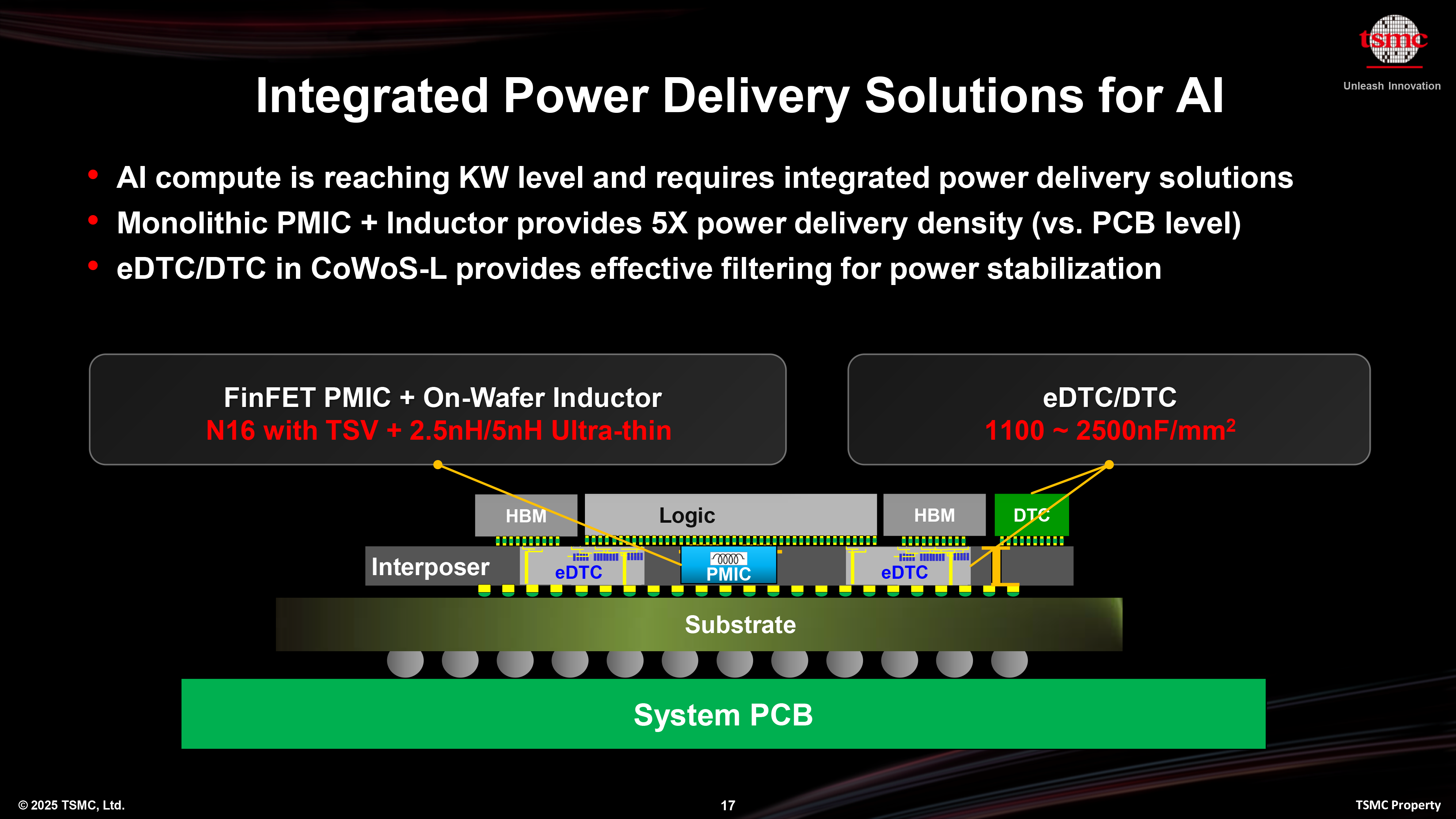
To address processors with kilowatt-class power requirements, TSMC wants to integrate monolithic power management ICs (PMICs) with TSVs made on TSMC's N16 FinFET technology and on-wafer inductors directly into CoWoS-L packages with RDL interposers, enabling power routing through the substrate itself. This reduces distance between power sources and active dies, lowering parasitic resistance and improving system-wide power integrity.
TSMC claims that its N16-based PMIC can easily handle fine-grained voltage control for dynamic voltage scaling (DVS) at the required current levels, achieving up to five times higher power delivery density compared to conventional approaches. In addition, embedded deep trench capacitors (eDTC/DTC), built directly into the interposer or silicon substrate, provide high-density decoupling (up to 2,500 nF/mm^2) to improve power stability by filtering voltage fluctuations close to the die and ensure reliable operation even under rapid workload changes. This embedded approach enables effective DVS and improved transient response, both of which are critical for managing power efficiency in complex, multi-core, or multi-die designs.
In general, TSMC's power delivery approach reflects a shift toward system-level co-optimization, where power delivery to silicon is treated as an integral part of the silicon, packaging, and system design, not a separate feature of each component.
Form-factor and cooling
The move to much larger interposer sizes will have consequences for system design, particularly in terms of packaging form factors. The planned 100×100 mm substrate is close to the physical limits of the OAM 2.0 form factor, which measures 102×165 mm. The subsequent 120×150 mm substrate will exceed these dimensions, likely requiring new standards for module packaging and board layout to accommodate the increased size.
Beyond physical constraints and power consumption, these huge multi-chiplet SiPs generate an enormous amount of heat. To address this, hardware manufacturers are already exploring advanced cooling methods, including direct liquid cooling (a technology already adopted by Nvidia for its GB200/GB300 NVL72 designs) and immersion cooling technologies, to handle the thermal loads associated with multi-kilowatt processors. However, TSMC can't address that problem on the chip or SiP level — at least for now.
Follow Tom's Hardware on Google News to get our up-to-date news, analysis, and reviews in your feeds. Make sure to click the Follow button.

Anton Shilov is a contributing writer at Tom’s Hardware. Over the past couple of decades, he has covered everything from CPUs and GPUs to supercomputers and from modern process technologies and latest fab tools to high-tech industry trends.
-
qxp Cerebras has been building wafer-scale computers for a while:Reply
https://www.cerebras.ai/chip -
hotaru251 gotta imagine the cost for that would be given how high the risk of defects are on such a large oneReply -
qxp Reply
The cost is not small, but that's because you are buying a whole wafer and it is a unique product. They work around defects by disabling some cores. The unique part is not just the more compact design, but also computational features, such as more bandwidth per operation. This can be a winning point if you compare it to GPUs, but, of course, the higher priced AI GPUs use HBM and negate some of the advantage.hotaru251 said:gotta imagine the cost for that would be given how high the risk of defects are on such a large one
Also, some defects are introduced when the wafer is cut, so using uncut wafer results in smaller defect rate. -
edzieba Reply
Tesla, too. Also fabbed by TSMC.qxp said:Cerebras has been building wafer-scale computers for a while:
https://www.cerebras.ai/chip
And as that article shows, TSMC announced SoW almost exactly a year ago (minus 1 day). With 2024 being a leap year, this could be an article entered into Toms' CMS with an off-by-one in the Year field. -
TJ Hooker I think Cerebras is a bit different, as their WSE is a monolithic piece of silicon fabbed from a single wafer. Tesla Dojo, and what is being discussed in this article, are bonding a bunch of separate chips onto a roughly wafer-sized package.Reply -
fiyz Installing that chip is probably the only time I would ever consider wearing an esd strap.Reply -
bit_user Reply
Tesla and Cerebras are different. Tesla stacks sub-reticle dies on a carrier, while Cerebras never cuts the dies out of the wafer, in the first place.edzieba said:Tesla, too. Also fabbed by TSMC.
Like TJ said.
