TSMC SVP Kevin Zhang opens up on process technology development & evolving demands: Interview
How 'everyone's foundry' adapts to demand
We had the opportunity to interview TSMC's Kevin Zhang, the deputy co-COO and SVP at TSMC, to discuss the latest trends in the semiconductor industry and how they impact TSMC's strategy moving forward.
Since its founding in the 1980s, TSMC's business strategy has been to meticulously fulfill the needs of its customers, transforming itself in accordance with the ever-evolving semiconductor landscape. In the coming years, the needs of the company's clients will become so diverse that it will offer different leading-edge production capabilities for segment-specific needs, marking a major milestone in its 'Everyone's Foundry' ideology.
Everyone's Foundry
Historically, processors for PCs were the driving force behind the industry's transition to next-generation chip manufacturing technologies. Then the smartphone revolution changed the rules of the game, and mobile SoCs became the alpha users of TSMC's (and the industry's) leading-edge fabrication processes.
The rise of AI once again changes everything, as data center-grade processors are about to become key adopters of TSMC's leading-edge nodes. However, as consumer devices still demand more performance and functionality every year, they also require a new process technology every year. As a result, TSMC has reached a point where it must offer different leading-edge technologies to meet highly distinctive needs. This is in addition to offering advanced packaging technologies for client and AI/HPC applications.
Article continues belowThese are some of the things we have learned from our interview with Kevin Zhang, Senior Vice President and co-COO, who is responsible for TSMC's technology roadmap, business strategy, and key customer engagement.
The road ahead
As users' needs change, semiconductor technologies follow. In the coming years, the industry will require three distinct offerings from contract chipmakers in general, and TSMC in particular.
The trend is moving in three directions:
- Maximum transistor density and performance efficiency.
- Maximum performance efficiency with the best possible power supply at reasonable costs.
- Multi-chiplet packaging solutions for data centers.
To address these distinct demands, TSMC is aligning its technology roadmap around three complementary directions: advanced transistor scaling, optimized power delivery, and leadership in multi-die system integration.
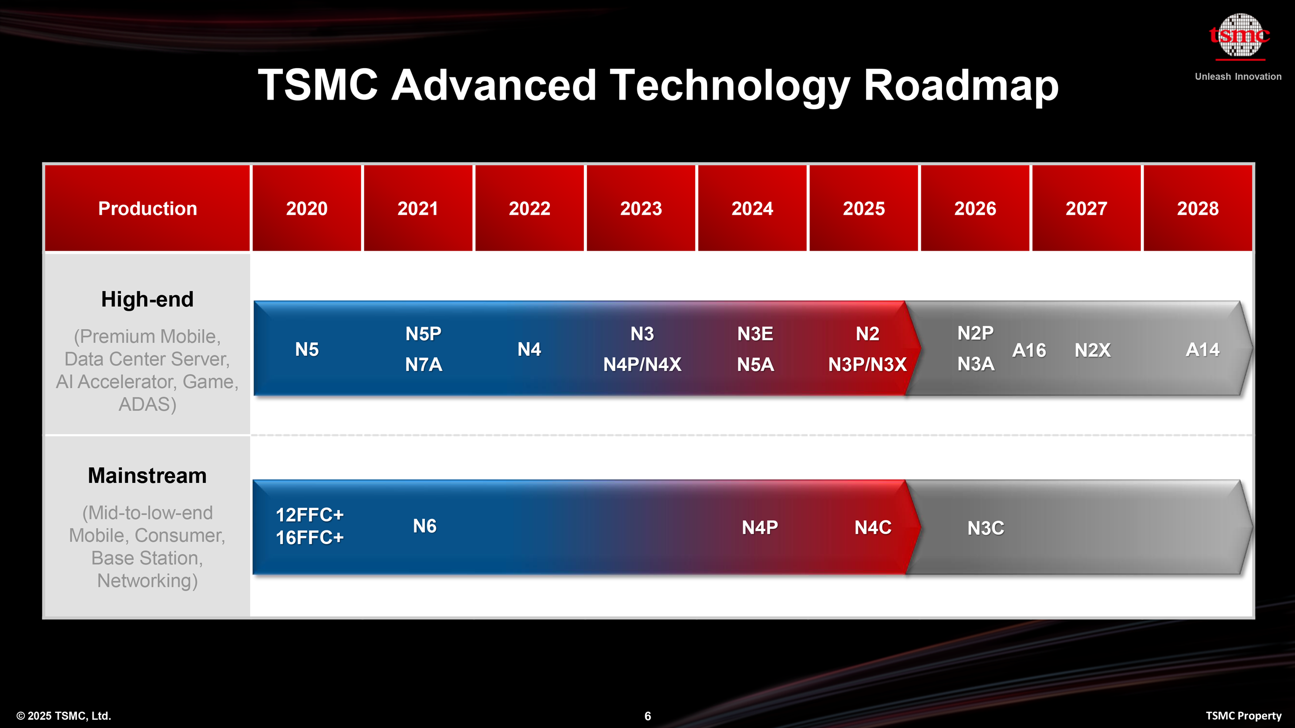
For products that require maximum performance efficiency, such as smartphones and PCs, TSMC will offer its N3P, N2, N2P, and A14 process technologies. These nodes are optimized for strong performance-per-watt without the complexity and cost of backside power delivery, enabling efficient scaling for mobile and consumer SoCs where area efficiency and battery life are critical.
For data center processors that consume a kilowatt or more of power, TSMC intends to offer A16 with Super Power Rail Backside Power Delivery Network (BSPDN) in late 2026, followed by A14 with SPR in 2029.
Also, to meet the growing need for multi-chiplet packaging solutions for data center-grade AI infrastructure, TSMC has expanded its advanced packaging portfolio, which includes silicon photonics, and embedded power components, into cohesive, high-bandwidth, energy-efficient systems.
Moore's law is (not) dead
Anton Shilov: Let's start with a rehashing of a traditional question that you hear quite often these days, and this concerns Moore's Law and whether it is alive or dead. With the transition from N5 to N3, we saw mixed chip density increased by around 30%. With the transition from N3 to N2, we can expect a 15% increase in transistor density. For A16, the expected increase is between 7% and 10% (the key feature of A16 is backside power delivery, rather than reworked transistors). Will we continue to witness diminishing returns when it comes to scaling (of transistor density) with every new node going forward, or will there be breakthroughs?
Kevin Zhang: If you look at the 5nm to 3nm to 2nm, and now to A14. The trend right now, we see power efficiency [improvements] of about 30% per generation. This is a kind of trend. We are seeing we are able to continue to drive transistor density aggressively in a ballpark with 20% per generation. So, performance [gains], we are talking about 15%. So those are the numbers I think are consistent with past generations. Going forward, beyond A14, I can say based on what we see, we have loads of innovations [incoming], so we can leverage that trend to continue beyond A14.
Anton Shilov: Now that you mentioned A14, you mentioned that it provides full node scaling benefits due to some technological breakthroughs, and you also mentioned the 2nd-Generation GAA nanosheet transistors. Does this mean that the breakthrough involves things like new materials, or something like this?
Kevin Zhang: I do not want to get into a specific innovation scheme at this point. Our technology team may publish a paper down the road at IEDM, I will let them to talk about. I have to tell you [changes from N2/A16] are quite substantial. From what we see today, we have full confidence to deliver A14 into high volume production in 2028 with substantial geometry scaling. So, I think it will really allow customers to harvest the intrinsic technology scaling benefits.
Every application needs its own node
Anton Shilov: When you announced A16, you said that backside power delivery was especially beneficial for AI HPC designs. In one of your interviews, you noted that smartphone SoCs can continue using process technologies without backside power delivery. Will your customers continue to be able to use next-gen nodes like A14 and A12 without a backside power delivery network (BSPDN)?
Kevin Zhang: I think we see some bifurcation for mobile applications, for example, where the power consumption is not that significant, compared to high-performance computing (HPC) [processors that] consume like a thousand or multiple thousand watts per die, per chip, or per package. We think mobile application customers continue to want to have a front side power delivery that is sufficient to achieve power, performance, and cost benefits. So, that's why you see we have N2 technology, we have A14, which does not have backside power delivery or Super Power Rail (SPR).
But as I mentioned earlier, a year after A14, we will have a version of [this] technology with the Super Power Rail [for] HPC applications. Your observation is correct, we are going to provide both technology tracks to allow different product segments to achieve their own optimization point.
Anton Shilov: Does it mean that going forward, your process technologies will get more tailored for a particular application?
Kevin Zhang: I think you can put in that way: our technology platform [will be] tailored for different applications. This is already happening today. You see mobile, we have a different optimization point. This is happening at the whole level as a design class level.
You see the transistor library, for example. We have different transistor libraries optimized for different product configurations, different product applications. At the transistor technology level, you talk about the Super Power Rail, and then you look at a package, we also have a different optimization point. You see, CoWoS is largely leveraged by HPC or AI applications. Then you look at the InFO [packaging technology], which is heavily leveraged by mobile customers. So yes, we already optimized our technology explicitly for different product segments.
Anton Shilov: Back in the day, you developed those HPC-oriented X process technologies like N4X, N3X, and now N2X. But starting with A16, they are already optimized for HPC from the start, is that correct?
Kevin Zhang: That is correct. A16 with Super Power Rail is really tailored for HPC applications. However, with the X-lineup — N4X, N3X, and N2X — we really try to enable customers to achieve maximum speed for single-thread applications.
Note: TSMC tends to offer multiple iterations of process technologies within one PDK (for example, N5, N5P, N4, N4P, or N3B, N3E, N3P). This enables the foundry to use expensive equipment for as long as possible, and also enables TSMC's customers to reuse their IP for as long as possible.
Anton Shilov: Now that it gets more expensive to transit from one node to another, do you expect the number of iterations within one generation to increase, or stay at around three or four? Will there be any specific questions of A16 or A14?
Kevin Zhang: If you look at the roadmap, you can count how many derivative versions of each major node we introduced, right? I mean, you use the 3nm example; you already see that there is N3E, N3X, N3P, and now we have N3C. So, we already have four different major flavors. But I do want to point out one thing: they are different derivative versions of [one] technology, they are compatible. For example, N3E to N3P to N3C, customers can reuse much of the design. You might need to characterize [chip design] a little bit differently because of certain things we optimize. But largely, the physical design can be reused directly. This allows our customer to basically leverage their previous product design or previous IP to achieve further optimization based on the process enhancement or process optimization.
Anton Shilov: So, going forward, starting from A14 and A16, are they going to offer those specialized versions as well?
Kevin Zhang: The Super Power Rail introduced quite new features because the power connection is totally moved from the front to the back. So, it does require a quite significant new design. That is a uniqueness of A16. When you move the power to the backside of the wafer, on the front side, much of the cell library [can be re-used] by applying some of the minimum changes. The changes largely happen on how you hook up the power.
Anton Shilov: But starting from A14, which is a brand-new node, do you plan to offer further iterations of this technology like you do today?
Kevin Zhang: I can tell you we continue to follow what we have done in the prior generations, like the 2nm, with A14. I would not be surprised [if] next year we are talking about the A14P or A14X. There will be A14C at some point. All of these are going to follow a similar philosophy [of current offerings]: to make it compatible, to make it incremental, and allow our customers to harvest the benefit of the investment that they have put in 14A when they make that transition.
Anton Shilov: Now that you have mentioned the C variants of process technology, can you estimate the cost benefits of N3C?
Kevin Zhang: The product level cost benefit depends on specific product design, product configuration, but from pure intrinsic technology capability point of view, I am talking about an order of 10% cost benefit.
As requirements grow, chip designers adopt more advanced process technologies
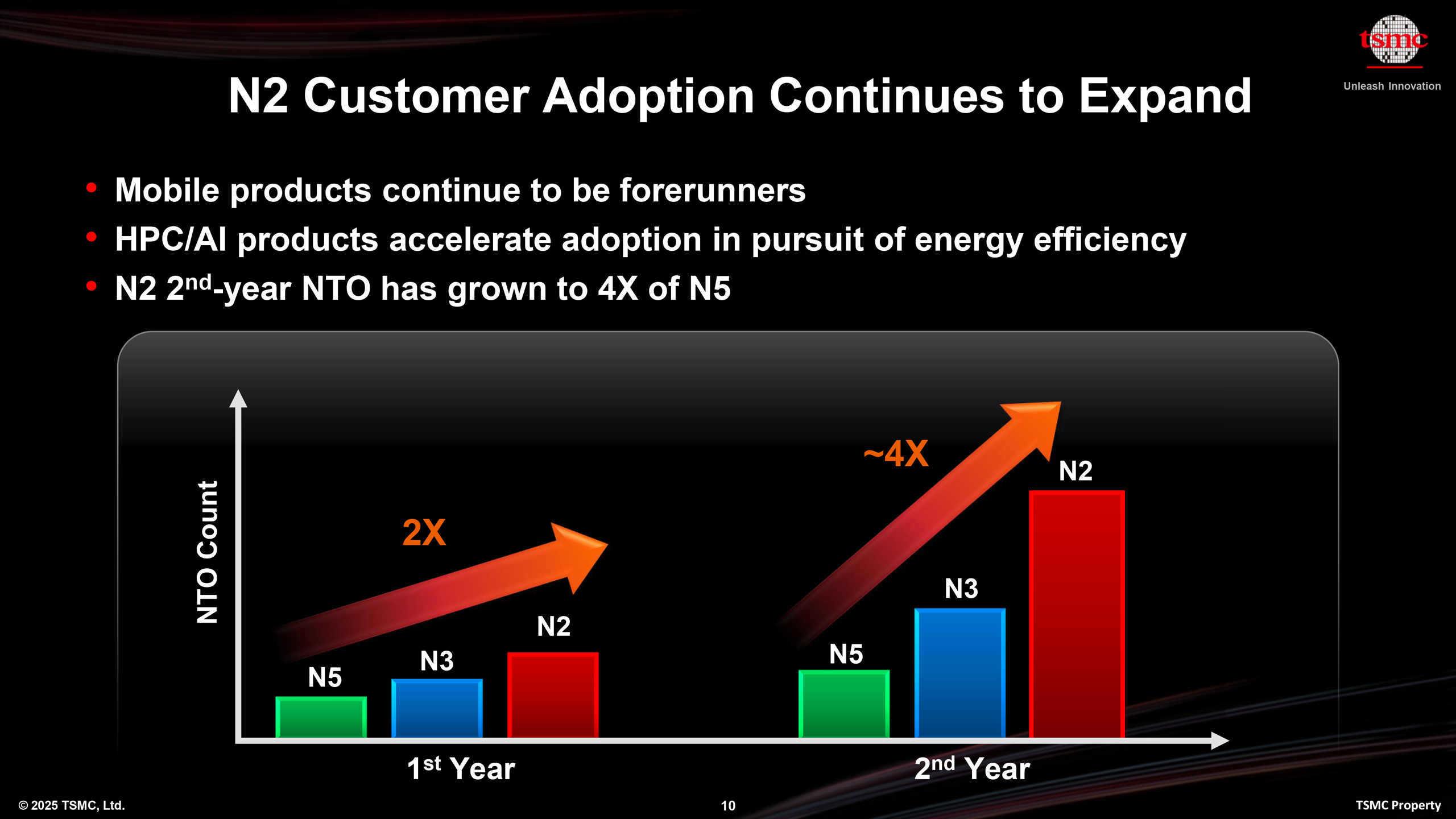
Anton Shilov: TSMC management has mentioned several times that the number of N2 tape-outs in the first two years is expected to be higher than the number of N3 and N5 tape-outs in their first two years, despite the fact that customers had to adopt all-new IPs for GAA process nodes. What are the reasons for that?
Kevin Zhang: Well, I think the main reason, it is driven by application. We talk a lot about AI these days. [But the] fundamental AI requirement is really energy-efficient compute, right? Whether it is a data center, whether it is edge devices. But you think about a data center, right? Today, data center's biggest single cost component is electricity, the consumed power. So, by adopting more advanced silicon technology, you bring power down substantially.
So, the customer sees a significant cost of ownership benefit by adopting more advanced silicon technology. So, this is really the underlying force for customers to be more aggressive in adopting advanced silicon technology nodes. Same things as they continue to incorporate more compute capability.
Think about the AI capability, for example, for a video. You know, the [video] you have taken [and uploaded to YouTube] needs extensive compute capability [from a Google datacenter]. So, all of these essentially drive the customer to go to a more advanced silicon, more advanced transistor technology.
So, we see that the trend is actually accelerating. That's why I showed that chart earlier. You see over the last three generations, the NTO number continue to increase, right? 2X for first year and the 4X for second year. So, this is really the reason behind those numbers.
Anton Shilov: Data center applications increasingly use a multi-chiplet design approach. However, when it comes to multi-chiplet solutions, we know that power consumption increases when a chip design gets disaggregated, so chip designers have to deal with this. But do you think you can help them cut the power consumption of their disaggregated designs on the foundry level?
Kevin Zhang: That is already happening today. Each specific function, elements, CPU, GPU AI neural engine, for example. They actually require a different optimization point. Today, we already offer many different flavors of transistors. For example, we allow a designer to use a different transistor for different function design optimization points today on the same die. They are already doing that. This is very important for us, to work with [a] customer to provide that specific optimization. So that's a monolithic design.
For multi-chiplet design, they actually can use drastically different silicon technology. Some, for example, use [the] most advanced technology, let's say 2nm for compute, but for low power, low speed elements, they can stay with a 3nm or even 5nm, or 4nm for that matter, and then leveraging our advanced integration scheme to bring them together. So, this is actually happening already today, at the system level we are working very closely with our different customers for different product applications.
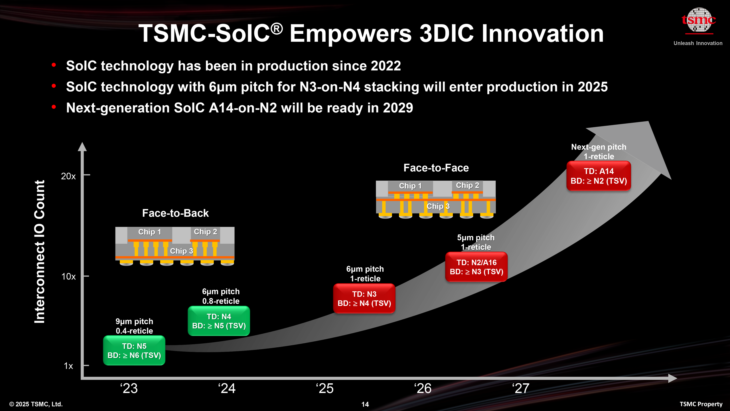
Note: Using different transistor libraries and process technologies can optimize power consumption. However, a multi-chiplet solution will still likely consume more power than an integrated solution. When it comes to 3D integration, TSMC's customers have to wait for the foundry to develop TSV versions of a process technology (e.g, N4 TSV, N3 TSV, N2 TSV, etc.) before this node can be used as a base die.
Anton Shilov: Last year, you talked about system-on-wafer integration for extremely powerful solutions. But how many customers are actually interested in such huge system-on-wafer level processors? Cerebras and Tesla, obviously. Are there many more?
Kevin Zhang: We see that trend, people continue to drive a larger interposer size to bring more compute units, more HBM. So that trend will continue. We see customer want to leverage wafer-level integration to address their future needs. But you know, this is probably a few years out because right now I talk about production CoWoS, it is 3.5X reticle size, in the future there will be 5X reticle size and 9X reticle size, and beyond 9X, wafer-level integration will become an important integration scheme. But they are still a few years out. But there are customers. You mentioned Cerebras and also Tesla's Dojo. They are more aggressive to leverage the wafer level integration.
TSMC will continue to evolve
With over 500 clients from different market segments, TSMC is evolving its strategy to address increasingly divergent customer needs by offering multiple, segment-optimized leading-edge manufacturing technologies for AI, HPC, and consumer applications and enabling its clients to reuse their IPs as its fabrication processes evolve. This once again emphasizes the company's long-standing 'Everyone's Fab' philosophy, shifting from a one-size-fits-all approach to a portfolio of purpose-built nodes and packaging solutions.
Going forward, TSMC will offer leading-edge process technologies with its Super Power Rail backside power delivery network (e.g., A16 and A14P) for AI and HPC applications; leading-edge nodes without BSPDN (e.g., N3P, N2, N2P, A14) for client and smartphone processors; and cost-optimized advanced nodes (e.g., N4C, N3C, N2C) for designs aimed at cost-sensitive applications.
Previously, the company offered its cost-optimized nodes only for mature nodes (e.g., N16FFC, N12FFC). For multi-chiplet and disaggregated designs, TSMC continues to expand its 3DFabric portfolio with diverse offerings for client/mobile (InFO), for AI and HPC 2.5D integration (CoWoS), for client and data center 3D integration (SoIC), and even system-on-wafer (SoW) integration for the most demanding solutions.

Anton Shilov is a contributing writer at Tom’s Hardware. Over the past couple of decades, he has covered everything from CPUs and GPUs to supercomputers and from modern process technologies and latest fab tools to high-tech industry trends.
-
thestryker Great read and managed to get some good answers to the questions asked. TSMC's BSPDN strategy is really interesting and it makes sense to me to silo it.Reply
Hopefully there will be some more details on packaging down the road as that's becoming as important as manufacturing process. -
hannibal And it tells that we still get speed upgrades, but also that those speed upgrades cost more.Reply
So performance / dollar does not get better now on. On the contrary. Somewhat interesting. In the past machines were expensive and did get cheaper when time gone past. Now the computer will become more expensive when time goes on...
Unless we stay in old cheaper nodes. Where we don´t get more speed, but the price neither does goes up as fast.

