Imec's next-gen high-speed chip transistor addresses manufacturing concerns — outer wall forksheet design simplifies production, but may sacrifice density
New design could inform CFET transistor production.

In 2017, imec introduced its forksheet transistor as a natural extension to gate-all-around (GAA) transistors. However, according to a recent announcement by imec at the VSLI Symposium 2025, there have been doubts about its manufacturability in high volumes. To address these concerns, the research giant has developed a new approach to bleeding-edge forksheet transistor design, which will enable the future of transistors to continue advancing.
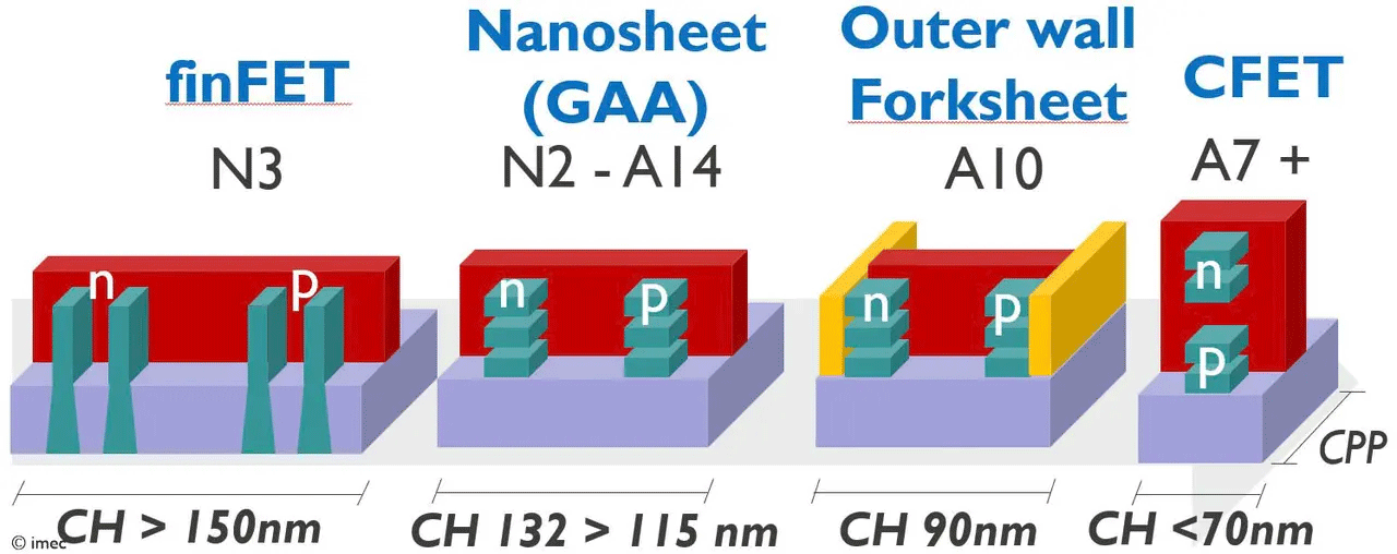
Researchers from imec introduced a new transistor layout named 'outer wall forksheet', which they expect to be used starting from the A10 generation (1nm, 10 Angstroms) all the way to the A7 generation, according to a new imec paper.
Knowledge gained from the volume manufacturing of these outer wall forksheet transistors could be useful for the production of next-generation complementary FET (CFET) transistors.
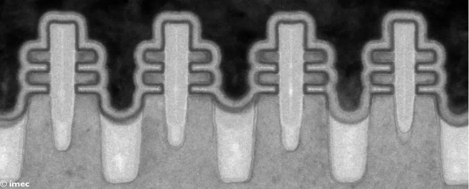
Leading chipmakers — Intel, TSMC, and Samsung — are transitioning from FinFET transistors to GAA transistors with their 18A, N2, and SF3E process technologies. GAA transistor structures allow currents to flow through horizontally stacked silicon layers, surrounded by material on all sides, thereby reducing leakage. This offers better control for performance and power consumption, as well as enabling smaller cell dimensions. However, scaling beyond three generations using this approach is difficult, according to imec.
The next major architecture — CFET — utilizes vertical stacking of n-type and p-type transistor types on top of each other, essentially allowing two transistors to fit within the footprint of one, while also boosting performance and reducing power consumption. However, CFETs are extremely hard to produce, so chipmakers and researchers like imec intend to use forksheet transistors as an intermediate step between GAA transistors and CFETs.
However, the initial version of the forksheet design, presented in 2017, appears to be too complex for manufacturing with acceptable cost and yields. Now, imec has presented a revamped version of its forksheet transistor design, which promises to be easier to manufacture while still providing power, performance, and areal benefits for next-generation process technologies.
The experience of manufacturing outer wall forksheet transistors at volume could inform the eventual transition to CFET over the course of the next decade. This could help outer wall forksheet transistors to not only serve as a bridge toward CFET, but also to inform how it might be manufactured.
Forksheet transistors
Forksheet transistors are meant to extend the capabilities of GAA transistors for several generations before CFETs inevitably take over at some point in the 2030s. The inner wall forksheet transistor design places a dielectric wall between (or beside) transistor channels to allow tighter placement of n-type and p-type devices, without electrical interference. This type of transistor design enables tighter spacing and more compact layouts while reusing many fabrication steps from existing nanosheet flows.
The original forksheet design — called inner wall forksheet — places the wall between nMOS and pMOS devices inside the standard cell, before gate patterning. However, while it may be effective on paper, this inner wall structure faced issues related to manufacturability.
To reach a 90nm cell height, the insulating divider of an inner wall forksheet needs to be extremely narrow, around 8 to 10nm. Since the wall is placed before gate patterning, it gets exposed to every further processing step, which may erode it. This puts strict requirements on the material used.
Additionally, placing selective features for n-type and p-type regions becomes difficult, as the mask must align exactly over the thin wall. In most circuits, both transistor types share a single gate, but the wall blocks this connection, unless the gate is extended over it, which adds unwanted capacitance.
Lastly, the inner wall forked gate only covers three sides of the channel, which weakens its control compared to GAA designs, especially as channel lengths shrink.
Given potential difficulties with manufacturing inner wall forksheets, the engineers at imec decided to redesign the layout and came up with what they call an outer wall forksheet.
This updated version relocates the insulating divider (or wall) to the edge, between adjacent standard cells. Instead of separating different polarities within one cell, it now separates same-polarity devices across cell boundaries. This layout enables the wall to be widened to about 15nm, without affecting the compact cell height.
It also allows the barrier to be built late in the process flow, after key steps such as source/drain formation and the nanosheet channel release step. As a result, the barrier avoids damage from earlier steps and can be constructed using well-established silicon dioxide material and tools.
Since the thickness of the wall is now 15nm, this likely affects transistor density, as outer wall forksheet devices are larger compared to inner wall forksheet transistors. However, the manufacturability and performance advantages that the outer-wall forksheet transistors offer may outweigh the potential advantages of the initial version.
Improved manufacturability
This change in sequence to introducing an outer wall offers two important benefits: simpler fabrication and better gate integration. The gate electrode can now link both transistor types, without needing to cross a barrier, which simplifies circuit design.
Furthermore, trimming the divider by a few nanometers during the final steps enables the gate to wrap around a larger portion of the channel. Simulations show that removing 5nm of the wall leads to approximately a 25% increase in drive current, due to improved electrical control, which will enhance performance.
Another advantage of the outer wall forksheet transistor is the improved ability to apply mechanical stress to the channel. During the early steps, a protective mask covers the region where the wall will be placed later. The silicon underneath this mask serves as a continuous crystal template for the surrounding growth of source and drain regions.
This continuous structure allows strain-inducing materials — such as silicon-germanium for p-type devices — to apply compressive stress directly into the channel, which boosts hole mobility and drive current, thereby improving performance.
Earlier designs, including both GAA nanosheets and the initial forksheet, lacked this strain continuity. Without a guiding structure, unwanted vertical mismatches formed during material growth, reducing the mechanical stress and harming performance. The new design avoids these defects, allowing consistent enhancement of current through strain techniques.
Promising results
Testing through simulated memory layouts and oscillator circuits confirmed the benefits, according to imec. In static memory cells, the new layout at A10 achieved a 22% area reduction compared to A14 nanosheet designs, due to tighter packing of like-type devices and a reduced gate pitch.
Oscillator results showed that, when full strain was applied, the new layout matched or exceeded performance of A14 and 2nm designs. Without strain, drive current dropped by roughly 33%.
Experience with manufacturing forksheet transistors is highly relevant to the development of CFETs as many of the process steps, materials, and design concepts overlap. Forksheet transistors place p-type and n-type devices next to each other. To contrast, next-generation CFETs stack two different transistor types vertically, though the base techniques are the same.
To that end, imec is now studying how this layout may be adapted for upcoming CFET designs. The researchers believe that its latest forksheet design may serve as a transition step for future vertical device architectures, enabling a smoother evolution path for next-generation process technologies.
Follow Tom's Hardware on Google News to get our up-to-date news, analysis, and reviews in your feeds. Make sure to click the Follow button.

Anton Shilov is a contributing writer at Tom’s Hardware. Over the past couple of decades, he has covered everything from CPUs and GPUs to supercomputers and from modern process technologies and latest fab tools to high-tech industry trends.
-
abufrejoval Thank goodness for imec (and ASML). If it wasn't for them, I'd just say this for EU high-tech and projects like the EPI : "could the last one leaving please turn off the light?"Reply
I've heard them talk about the vertically stacked N and P transistors perhaps 10 years ago and they reported temperature control and matching materials as the biggest manufacturing issue back then: I throught they had completely given up on that and am glad to hear that's still an ace up their sleeves.


