Intel and TSMC to Report on Next-Gen CFET Transistor Progress
Intel and TSMC to present papers covering complementary field effect transistors.

Intel and TSMC are set to unveil their progress on vertically-stacked complementary field effect transistors (CFETs) at the upcoming International Electron Devices Meeting (IEDM) conference, reports eeNewsEurope. CFETs are set to succeed gate-all-around (GAA) transistors (which yet have to take over the market themselves), probably sometime in the next decade.
The concept of CFETs, which involve layering n- and p- type transistors atop one another, was initially introduced by the IMEC research institute in 2018. While most early studies stemmed from academic circles, commercial companies like Intel and TSMC have now ventured into this arena and are actively exploring this next-generation type of transistor.
Intel
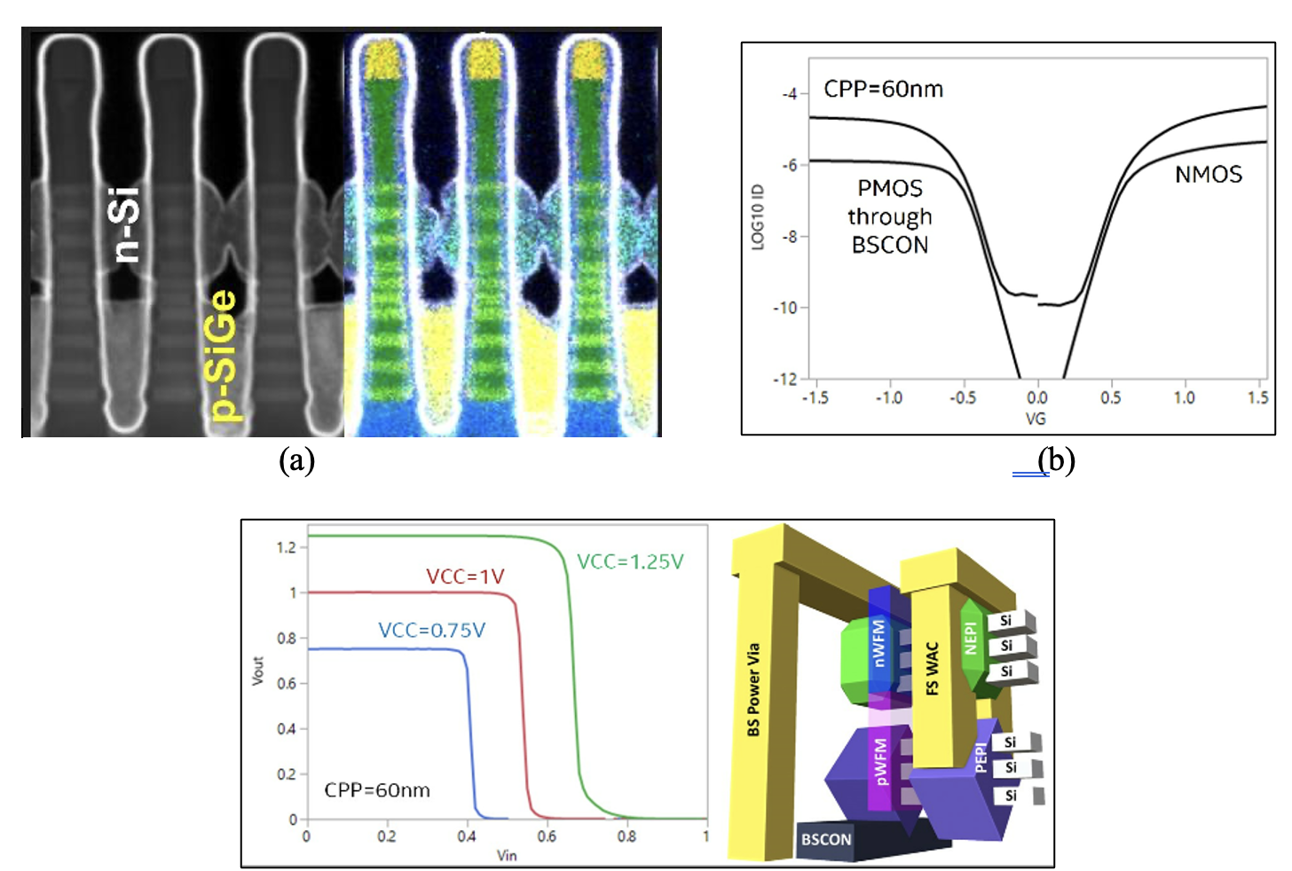
Intel's researchers have built a monolithic 3D CFET, which incorporates three n-FET nanoribbons layered above three p-FET nanoribbons, maintaining a vertical gap of 30nm. Intel's presentation titled "Demonstration of a Stacked CMOS Inverter at 60nm Gate Pitch with Power Via and Direct Backside Device Contacts" will describe functional inverter test circuits utilizing CFET at a 60nm gate pitch. This design also features vertically layered dual source-drain epitaxy and twin metal gate stacks, as well as incorporating the company's PowerVia backside power delivery.

TSMC
Not to be outdone by its rival, TSMC will discuss its hands-on CFET method, tailored for logic technology and featuring a 48nm gate pitch. The foundry's design accentuates layered n-type nanosheet transistors placed over p-type counterparts, boasting a remarkable on/off current ratio that spans six orders of magnitude.
TSMC's transistors have proven their durability, with more than 90% successfully enduring testing, according to the company. While the company admits that there are more features to be assimilated to fully harness CFET technology's capabilities, the ongoing work represents a pivotal step towards this objective.
Next-Gen Transistor
CFETs introduce a notable shift in transistor design, with their vertical stacking allowing for two transistors to fit within the footprint of one, thereby increasing transistor density on a chip. This design not only paves the way for enhanced space efficiency, but it also promotes a more streamlined CMOS logic circuit layout, facilitating improved design efficiency.
Additionally, the inherent structure of CFETs may lead to reduced parasitic effects, offering potential enhancements in performance and power efficiency. Their adaptable design capabilities, like the ability to balance NMOS and PMOS channel variations, combined with innovations such as backside power delivery, further streamline the manufacturing process, making CFETs a promising development in the realm of transistor technology.
Get Tom's Hardware's best news and in-depth reviews, straight to your inbox.
The efforts of both Intel and TSMC spotlight the importance of CFET technology for the future of the semiconductor industry.

Anton Shilov is a contributing writer at Tom’s Hardware. Over the past couple of decades, he has covered everything from CPUs and GPUs to supercomputers and from modern process technologies and latest fab tools to high-tech industry trends.
-
Diogene7 I don’t really understand why so much exponential technical and financial resources are allocated to attempt to maybe gain low performance / power efficiency incremental (10% / 15%) improvements on a technology, like silicon transistors, that is close to reaching its limit and is a dead end, versus re-allocating those resources to significantly invest in next generation computing technologies like spintronics related technologies (MRAM, Intel MESO concept, French R&D Lab Spintec FESO concept,…) as it seems that could improve power efficiency from 5x to 30x with plenty new opportunities (better suited for AI,…).Reply
The development of CFET is much too expensive compared to opportunities that spintronic related technologies would provide : CFET is unfortunately delaying a much better technology (spintronic technologies).
Also I don’t understand that at this stage DARPA and the US government (US CHIPS Act) still don’t yet make it a top priority fin order that the US regain its technological leadership…