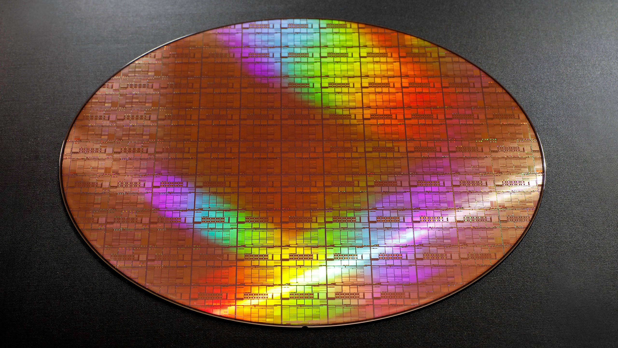
Japanese chipmaker Rapidus begins test production of 2nm circuits — company commits to single-wafer processing ahead of 2027 mass production target
PDK set to be available in Q1 2026.

Get Tom's Hardware's best news and in-depth reviews, straight to your inbox.
You are now subscribed
Your newsletter sign-up was successful
Rapidus on Friday announced that it had begun prototyping of test wafers with 2nm gate-all-around (GAA) transistor structures at its IIM-1 facility in Japan. The company confirmed that early test wafers are already attaining the expected electrical characteristics, which means that the company's fab tools operate as planned and its process technology development is proceeding well.
Test wafers flying over fab
Prototyping is an important milestone in semiconductor production that is meant to verify that early test circuits made using a new technology behave reliably, efficiently, and meet performance targets.
For now, Rapidus is measuring electrical characteristics of its test circuits, which includes parameters like threshold voltage (the voltage at which the transistor starts to conduct), drive current (how much current it can pass when switched on), leakage current (unwanted current flow when the transistor is off), and subthreshold slope (how sharply the device transitions from off to on). Other important characteristics include switching speed, power consumption, and capacitance. For obvious reasons, Rapidus does not share results, though the very fact that test wafers are flying around the fab is important.
Article continues belowThe IIM-1 site has seen rapid progress since construction began in September 2023. The clean room was finalized in 2024, and by June 2025, the company had connected more than 200 of its tools, including advanced DUV and EUV lithography tools. Rapidus installed advanced EUV tools in December 2024 and completed its first successful exposures with them by April 2025. By now, the fab is mature enough to run test wafers, enabling Rapidus to measure electrical characteristics of its GAA circuits to identify possible process issues and refine settings of tools or manufacturing steps.
Single-wafer processing for all steps
One interesting thing that Rapidus mentioned in its press release covering the announcement is that its IIM-1 fab will use the so-called single-wafer processing approach (a semiconductor manufacturing method in which each wafer is handled, processed, and inspected individually rather than in batches) for all front-end process steps.
Nowadays, large chipmakers like Intel, Samsung, and TSMC use a combination of batch and single-wafer processing methods in their semiconductor fabrication processes. Single-wafer processing is used for critical steps that demand precision, such as EUV and DUV patterning, plasma etch, atomic layer deposition, or defect monitoring. For other steps, such as oxidation, ion implantation, cleaning, and annealing, they process wafers in batches.
Rapidus plans to apply a single-wafer approach to all of its process steps, including oxidation, ion implantation, patterning, deposition, etching, cleaning, annealing, etc. Rapidus says that this enables precise control over each operation, as adjustments can be made specifically for the conditions or results observed on that single wafer. Since each wafer is treated independently, engineers can fine-tune parameters in real time, detect anomalies early, and quickly apply corrections without waiting for an entire batch to complete. As an added bonus, such a method generates larger amounts of high-resolution data per wafer compared to the mixed approach used by other chipmakers, which can be used to feed AI algorithms that monitor and optimize manufacturing conditions. These algorithms can potentially enable faster gathering of information for continuous process improvements (CPI) to reduce defect density and increase yields, as well as for statistical process control (SPC) to reduce performance variations. Also, single-wafer process systems make it easier to change settings and switch between small and large production runs, which is important for Rapidus, which aims to serve smaller makers.
Get Tom's Hardware's best news and in-depth reviews, straight to your inbox.
However, this method also introduces some trade-offs. Since wafers are processed one at a time, throughput per tool (well, some tools) is lower compared to batch processing, potentially extending production cycle times and making production more expensive. The equipment required is more complex and costly, and coordinating the movement of wafers across all steps individually adds overhead.
However, Rapidus believes that despite higher upfront costs and slower processing, the long-term benefits in defect reduction, yield improvement, and adaptive process control can make single-wafer processing a compelling strategy for the production of chips at 2nm and beyond.
PDK on track for Q1 2026
To support early customers, Rapidus is preparing to release the first version of its process development kit in the first quarter of 2026. The company is also working to provide the infrastructure needed for customer chip design prototyping at the IIM-1 site.
Follow Tom's Hardware on Google News to get our up-to-date news, analysis, and reviews in your feeds. Make sure to click the Follow button.

Anton Shilov is a contributing writer at Tom’s Hardware. Over the past couple of decades, he has covered everything from CPUs and GPUs to supercomputers and from modern process technologies and latest fab tools to high-tech industry trends.
-
thestryker It's really good to see this is hitting the appropriate timelines. I'm not totally sure how viable the long term will be if they try to keep up with leading edge, but they may be able to carve out a solid enough business just following slightly behind. Samsung has really fumbled the ball on execution and Intel ran into the irrationality of wall street. Nobody should want to be left with just TSMC as an option so hopefully Rapidus can continue to execute.Reply -
Notton Here's hoping it's not just words and they get this working. Projects run by the Japanese government haven't been confidence inspiring, nor successful for the past... 20~30 years. There's always someone that lies about results and embezzles funds when the government gets involved. You'd think they'd learn by now.Reply -
Mr Majestyk It would not surprise me to see them surpass Samsung in quick time, say 2030 and become the de facto second choice after TSMC.Reply -
duffer9999 I don't see how they are gonna make money using single wafer. If you batch process a boat of 24 wafers in an etch bath, for cleaning or etch, it may take 15 minutes. They would have to run 24 wafers through a bath individually. That would take 6 hours.Reply
