TSMC discloses N2 defect density — lower than N3 at the same stage of development
Two quarters before mass production.

Get Tom's Hardware's best news and in-depth reviews, straight to your inbox.
You are now subscribed
Your newsletter sign-up was successful
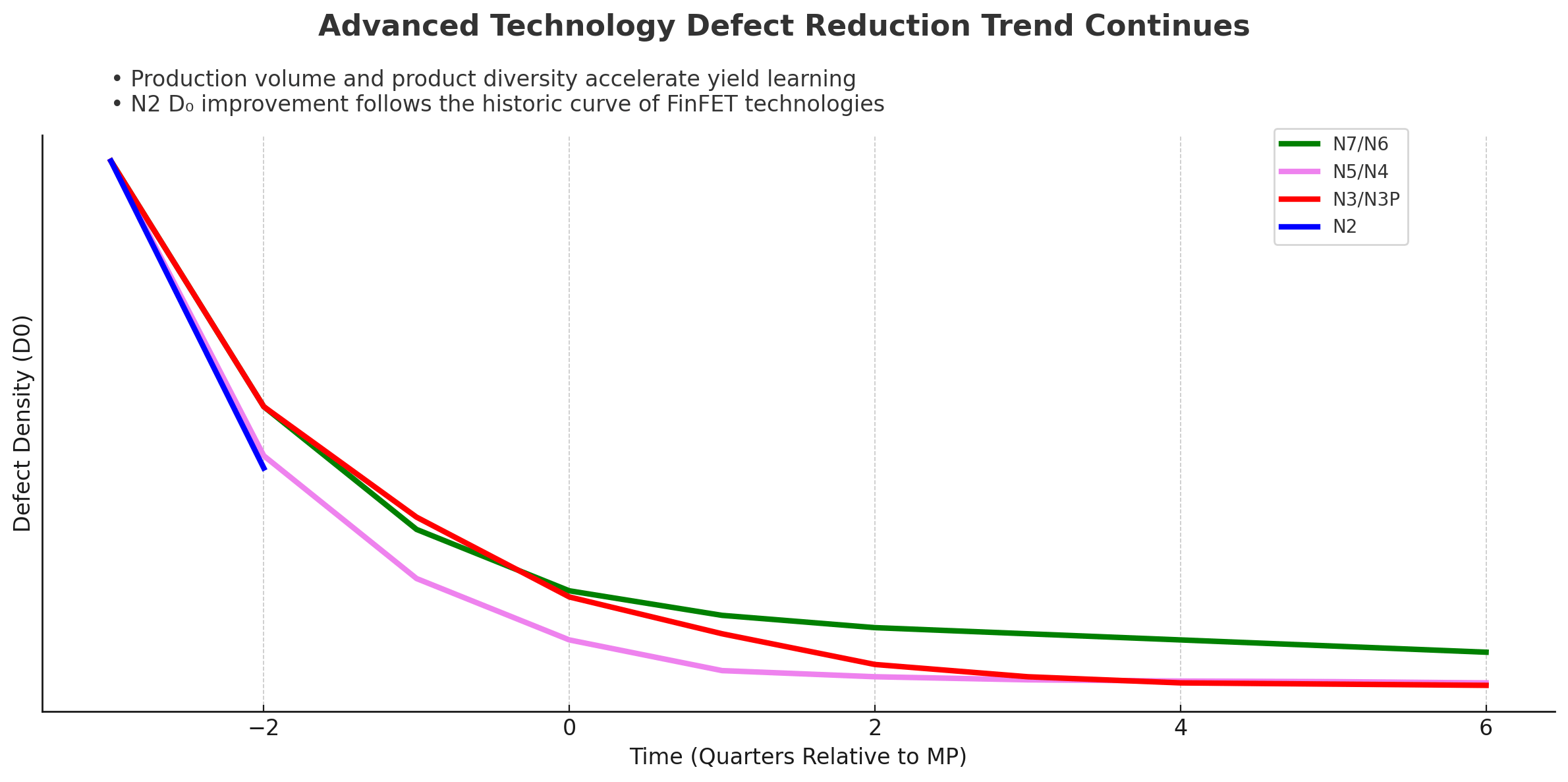
TSMC exposed the defect density (D0) of its N2 process technology relative to its predecessors at the same stage of development at its North American Technology Symposium this week. According to the company, the defect density is below that of N3, N5, and N7 manufacturing nodes. In addition, the slide published by ComputerBase reveals that N2 is two quarters away from mass production, which means that TSMC is on-track to start making 2nm-class chips in late Q4 2025, as expected.
Although TSMC's N2 is the company's first process technology to adopt gate-all-around (GAA) nanosheet transistors, the node has lower defect density than its predecessors at the same stage of development, two quarters before mass production (MP). The predecessors — N3/N3P, N5/N4, and N7/N6 — all relied on well-known FinFET transistors. So, despite being TSMC's first node using GAA nanosheet transistors, the N2 defect density is getting lower quicker (well, steeper) than that of its predecessors before the high volume manufacturing (HVM) milestone.
The chart plots defect density against time, spanning from three quarters before mass production through six quarters after MP. Across all nodes shown — N7/N6 (green), N5/N4 (violet), N3/N3P (red), and N2 (blue) — defect densities drop significantly as production ramps, though at different rates depending on node complexity. Notably, N5/N4 displayed the most aggressive early defect reduction, while N7/N6 showed a more gradual yield improvement. The N2 curve begins with higher initial defect levels than N5/N4 but declines sharply, closely matching the defect reduction trajectory of N3/N3P.
Article continues belowThe slide emphasizes that production volume and product diversity remain the key drivers for accelerating defect density improvements. Larger production volumes and a wide variety of products using the same process enable faster identification and correction of defect density and yield issues, enabling TSMC to optimize defect learning cycles. TSMC stated that its N2 fabrication technology got more new tape outs than predecessors (as TSMC now risks producing N2 chips for smartphone and HPC customers), so the defect density decrease curve mostly proves that.
The fact that N2's defect reduction rate aligns well with previous FinFET-based nodes is particularly significant, given the risk factors associated with introducing an all-new transistor architecture. It suggests that TSMC has successfully transferred its process learning and defect management expertise into the new GAAFET era without major setbacks (at least based on what TSMC discloses).
Get Tom's Hardware's best news and in-depth reviews, straight to your inbox.

Anton Shilov is a contributing writer at Tom’s Hardware. Over the past couple of decades, he has covered everything from CPUs and GPUs to supercomputers and from modern process technologies and latest fab tools to high-tech industry trends.
-
usertests Everyone be hating on N3, but it's going to stick around for the next 10-20 years as the last TSMC FinFET node, so they can fix it up gradually.Reply -
thestryker Reply
I don't think it was bad by any means, but they'd gotten too aggressive with SRAM scaling which caused yield issues with the first version. It's still a good node (and I'm sure all of the derivatives after N3E will be great) aside from clock scaling, but that seems to be an issue with TSMC's nodes in general.usertests said:Everyone be hating on N3, but it's going to stick around for the next 10-20 years as the last TSMC FinFET node, so they can fix it up gradually. -
dalek1234 So TSMC discloses n2 defects density when compared to previous node, which Intel hides theirs. Got it.Reply -
abufrejoval Reply
I agree that this seems to be a slightly obfuscated message aimed at decisive people in the know designed to tilt some rather political decisions.dalek1234 said:So TSMC discloses n2 defects density when compared to previous node, which Intel hides theirs. Got it.
Unfortunately I personally don't have the foggiest as to what this actually means.
