TSMC reiterates it doesn't need High-NA EUV for 1.4nm-class process technology

ASML
(Image credit: ASML)

TSMC reiterated its long-known stance on next-generation High-NA EUV lithography tools at its European Technology Symposium in Amsterdam. The company does not require these highest-end lithography systems for its next-generation process technologies, including A16 (1.6nm-class) and A14 (1.4nm-class) process technologies. To that end, TSMC will not adopt High-NA EUV tools for these nodes. 

" People seems to always interested when TSMC going to use High-NA, I think our answer is very simple," said Kevin Zhang, Deputy Co-COO and Senior Vice President of Business Development and Global Sales, at the event. "Whenever we see High-NA will provide meaningful, measurable benefit, we will do it. With A14, the enhancement I talked about earlier is very substantial without using High-NA. So, our technology team continues to find a way to extend the life of current EUV while harvesting the scaling benefit."

TSMC's A14 process relies on the company's second-generation nanosheet gate-all-around transistors, along with a new standard cell architecture. According to TSMC, A14 provides up to 15% higher performance at the same power and complexity, or alternatively, 25% to 30% lower power consumption at the same frequency. In terms of transistor density, A14 achieves a 20% increase compared to N2 for mixed logic/SRAM/analog configurations and up to 23% when it comes to pure logic.

Such performance, power, and transistor density increases represent the so-called 'full node advantage', and yet, TSMC does not need next-generation High-NA EUV lithography tools to produce chips with predictable yields and desired performance and power characteristics on its A16 and A14 process technologies. One should keep in mind that TSMC's A16 is essentially N2P with a Super Power Rail (SPR) backside power delivery network. As TSMC does not need High-NA EUV tools for N2 and N2P, it will not need them for A16 either. By contrast, A14 is an all-new node that will be used for mass production in 2028, so the fact that TSMC does not need High-NA for this one is quite remarkable.

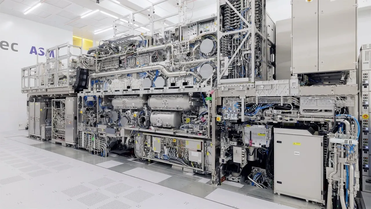
When asked whether A14 heavily relies on multi-patterning, Zhang responded that he could not comment on specifics, but said that TSMC's technology team had found a way to produce chips on a 1.4nm node without using High-NA EUV tools that provide an 8nm resolution compared to a 13.5nm resolution of Low-NA EUV systems.

"This is a great innovation from our technology team," said Zhang. "As long as they continue to find a way, obviously, we do not have to use High-NA EUV. Eventually, we will use it at some point. It is just so we need to find a right interception point, provide the maximum benefit, maximum return on investment."

It is noteworthy that TSMC's A14 will be succeeded by A14 with SPR backside power delivery in 2029, and it does not appear that the foundry will require High-NA EUV tools for this iteration either. To that end, it looks like, unlike Intel, which is set to start using next-generation EUV lithography machines with its 14A manufacturing technology to reduce the number of EUV exposures (read: multipatterning) and process steps in 2027 – 2028, TSMC has no plans to use High-NA EUV for mass production until at least 2030, or perhaps even later.

Follow Tom's Hardware on Google News to get our up-to-date news, analysis, and reviews in your feeds. Make sure to click the Follow button.

TOPICS
Anton Shilov
Contributing Writer

Anton Shilov is a contributing writer at Tom’s Hardware. Over the past couple of decades, he has covered everything from CPUs and GPUs to supercomputers and from modern process technologies and latest fab tools to high-tech industry trends.

  • kjfatl
    TSMC doesn't need it.
    Intel does, for a good reason.

    TSMC has a lot of EUV capacity in place and has a lot invested in this equipment. It's like having a fleet of cars with 70,000 miles on them. They will likely go down the path of double and triple patterning to get small features. Not only that, the High NA equipment wont' fit in their existing fabs.

    Meanwhile, Intel has very little EUV capacity. For Intel, the only sane thing to do is to invest in the next generation equipment. They need to build completely new fabs, so the size of the equipment isn't an issue. They won't really need High NA for 4 or 5 years, but they will keep the equipment running for 20 years or more. In the meantime, they will have the option of doing single patterning on high volume product to decrease process time and cost.
    Reply
  • rluker5
    Intel said the same thing with not needing EUV for 10nm.
    In the end they didn't, but it wasn't pretty getting there.
    Reply
  • ak47jar3d
    I wonder if 1.4 nanometer will be the end. How much can you keep shrinking transistors? The limit seems close but that is merely speculation.
    Reply
  • rluker5
    ak47jar3d said:
    I wonder if 1.4 nanometer will be the end. How much can you keep shrinking transistors? The limit seems close but that is merely speculation.
    1.4 is the beginning for High NA EUV. But they really aren't 1.4nm. Also High NA has reduced reticle size to go along with it's increased precision so it isn't all good news.
    Reply
  • ak47jar3d
    rluker5 said:
    1.4 is the beginning for High NA EUV. But they really aren't 1.4nm. Also High NA has reduced reticle size to go along with it's increased precision so it isn't all good news.
    The Name would have tricked me. Its seems crazy that they can even make 1.4 nm work.
    Reply
  • russell_john
    What no one is mentioning is EUV technology is owned and licensed by the US Government. Imagine sinking billions more into the new technology only to have a wannabe world dictator like Trump yank that license away because you hurt his feelings?

    Bottom line is the main reason they aren't going forward with this is because no other nations trust the US Government anymore to not do knee jerk things
    Reply
  • thestryker
    All of the articles about TSMC and High-NA keep emphasizing the cost of just buying the machines, but I'd be surprised if that has much to do with it. High-NA EUV machines are much larger and heavier than EUV machines while requiring more power. While I doubt this means much of anything for TSMC's newest fabs it's a big problem for the rest. Retrofitting isn't a simple prospect and nobody is doing1:1 EUV replacements because the overall economics of only using High-NA don't work out yet.
    Reply
  • usertests
    ak47jar3d said:
    I wonder if 1.4 nanometer will be the end. How much can you keep shrinking transistors? The limit seems close but that is merely speculation.
    The names are fake. Pay them no heed.

    There are more technologies that haven't been deployed yet. TSMC is making GAAFETs now, but we will see at least 1-2 variations of GAAFETs that are expected to be superior. For example, complementary field-effect transistors (CFETs).

    3D stacking and packaging will become as big of a deal as the nodes themselves. Large amounts of cache/memory will be migrating into 3D layers in CPUs, and if they figure out how to have many CPU layers without melting chips, that will happen and processors will grow vertically like V-NAND did.
    Reply
  • phead128
    rluker5 said:
    Intel said the same thing with not needing EUV for 10nm.
    In the end they didn't, but it wasn't pretty getting there.
    High-NA is an optical (lens) optimization of Low-NA EUV. It's nowhere near the huge gap between Low-NA EUV and DUV which Intel preferred for 10nm.

    Intel hasn't even mastered Low-NA EUV, High-NA is no silver bullet if you cant even master the low version.
    Reply