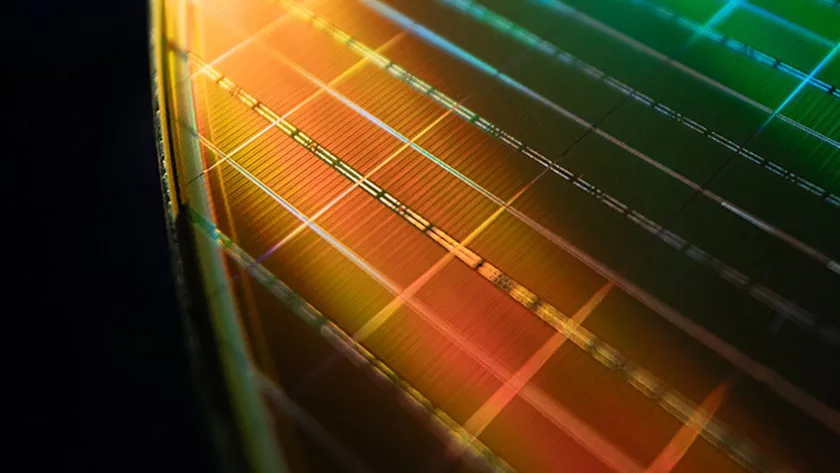
Latest about High NA EUV
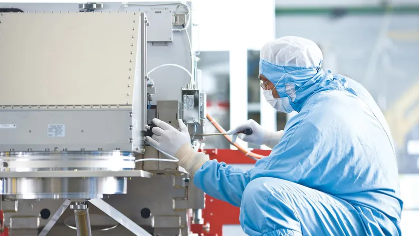
Premium ASML, Intel, Samsung, and TSMC back development of 6×12-inch to build large processors using High-NA EUV lithography systems without stitching.
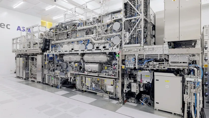
TSMC discloses plans to use High-NA EUV lithography in 2030, 6×12-inch photomasks with new scanners in 2033.

Intel is leading the semiconductor industry with High-NA fleet and process-maturity milestone as it reaches 1 million wafers processed using High-NA tools, moves forward with 6×12 photomask effort.

Samsung Foundry's plans change significantly from the 2024 roadmap.

Premium Low-NA, high stakes

Intel is using ASML’s High-NA EUV tools to pattern select Panther Lake layers, marking the technology’s first use in high-volume logic production

Intel begins expansion of its Bowers Campus in Santa Clara to produce more photomasks in-house, which is set to be crucial as process technologies get more sophisticated.

ASML to use a new CO2 laser system and tin droplet generator to increase EUV light source performance to 1000W and lithography tool productivity to 330 wafers per hour in 2030 and beyond.