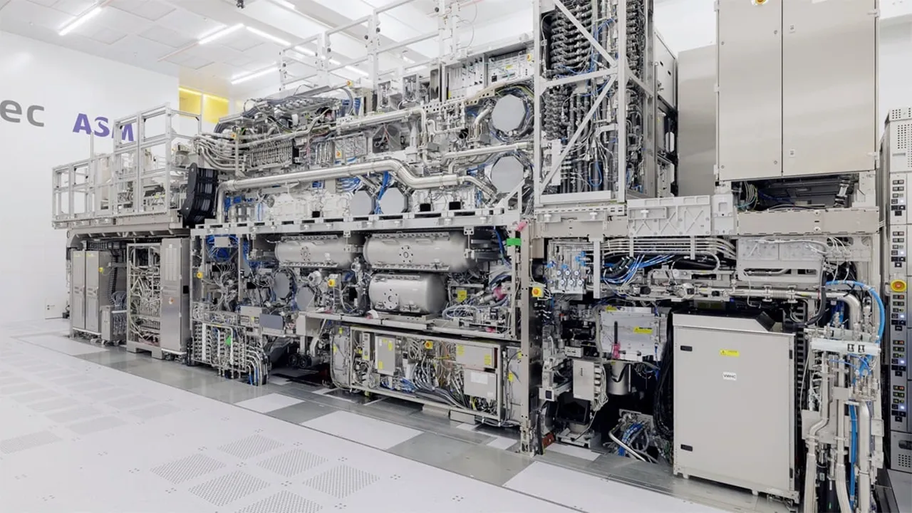
Intel announced that it had installed ASML's Twinscan EXE:5200B, the industry's first High-NA lithography tool with 0.55 numerical aperture projection optics made for commercial chip production. The tool has passed acceptance testing and will be used for development of Intel's 14A fabrication process, which will be the world's first node to rely on High-NA EUV scanners for its most critical layers. The achievement indicates that High-NA EUV lithography is moving beyond early experimentation toward high-volume manufacturing (HVM).
ASML's Twinscan EXE:5200B builds on the 1st Generation EXE:5000 platform that Intel received in 2023 for its Oregon R&D fab. The new tool can 'print' chips with an 8nm resolution, enabling scaling beyond which is currently possible with Low-NA EUV tools that offer a 13nm resolution without using multi-patterning. Unlike the EXE:5000, the EXE:5200B is capable of processing 175 wafers per hour at a 50 mJ/cm² dose (up from 185 wafers per hour at at a 20 mJ/cm² dose) and achieves overlay accuracy of 0.7 nanometers, a critical parameter as feature dimensions continue to shrink.

To boost performance, the scanner integrates a higher-power EUV light source to enable faster wafer exposures at a 50 mJ/cm² dose. This in turn supports workable resist/process windows with strong image contrast while minimizing line-edge roughness (LER) and line-width roughness (LWR), which tend to be challenging with modern production nodes.
Article continues belowASML and Intel did not limit their work to the optics and light source. They also reworked the wafer stocker system, which is responsible for how wafers are stored, queued, and moved in and out of the scanner. For next-generation tools, this component of the system has a direct impact on both productivity and patterning accuracy.

The updated stocker design improves lot flow and wafer handling to make sure that wafers arrive at the exposure stage in a more predictable state. At the same time, it provides tighter thermal control, keeping wafers and carriers at stable temperatures before and after exposure, an important factor as even tiny temperature variations can cause wafer expansion or contraction, leading to overlay errors, which in turn leads to an increase in defects and decrease of yields.
In addition, by reducing thermal and mechanical variation, the new architecture helps to minimize drift over long runs, thus enabling the scanner to maintain stable behavior and reducing the necessity for frequent recalibration. This stability will be particularly important for multi-pass and multi-exposure patterning, which will be inevitably used in the coming years for sub-1nm process technologies.
One of EXE:5200B's parameters that is hard to overestimate is its overlay performance of 0.7 nm, which was achieved by advancements of stage control, sensor calibration, and environmental isolation. Overlay performance is crucially important for next-generation process technologies as even tiny alignment errors can translate into yield losses.

It is necessary to note that ASML's Twinscan EXE:5200B is not just another EUV scanner in Intel's fab, but rather a foundation that is expected to enable Intel to regain its leadership in the semiconductor industry.
To use the new lithography tool, Intel is conducting parallel work on masks, etch processes, resolution enhancement techniques, and metrology that must be co-optimized to extract the maximum value from High-NA EUV patterning.
Intel says that its High-NA tools will enable more flexible design rules, reduce the number of patterning steps, lower mask counts, shorter cycle time, and increased yields thanks to lack of multipatterning with 14A and more advanced process technologies. Meanwhile, as Intel learns how to use High-NA EUV tools and gains valuable HVM experience, it will be able to insert High-NA EUV multi-patterning when it needs to in the sub-1nm era without significant effect on yields.

Follow Tom's Hardware on Google News, or add us as a preferred source, to get our latest news, analysis, & reviews in your feeds.
