
New 1.4nm nanoimprint lithography template could reduce the need for EUV steps in advanced process nodes — questions linger as no foundry has yet committed to nanoimprint lithography for high-volume manufacturing

Japan’s Dai Nippon Printing (DNP) claims to have developed a nanoimprint lithography template capable of patterning logic with a feature size of 1.4nm, with plans for mass production in 2027. Canon, which has spent years pursuing nanoimprint lithography as a lower-power alternative to EUV, is already shipping its first 300mm tools to early research partners.
Together, the companies are pointing to imprinting as a way to cut lithography power consumption by up to 90% for advanced nodes. With TSMC and Samsung preparing for 1.4nm mass production within the next few years, DNP’s announcement comes just as EUV’s cost and energy demands are escalating the fastest in leading-edge fabs. The technology promises a dramatic shift in the economics of chipmaking, but whether it can meet the defectivity, overlay, and throughput requirements of high-volume logic remains an open and pressing question.
Skyrocketing energy use
The industry has grown accustomed to talking about how much power finished AI chips consume, yet the energy needed to fabricate those chips has grown at a comparable pace. EUV scanners each consume as much power as a small city — 1,400 kilowatts per tool — meaning that modern fabs that run several dozen EUV units must reserve enormous electrical capacity before a single wafer is exposed. This rising power use is compounded by the fact that shrinking features below 2nm increase the number of passes and exposures required, raising energy consumption per wafer for next-gen high-NA EUV.
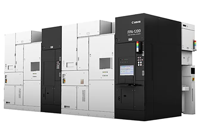
Canon, which has long argued that the industry needs an alternative, offers a nanoimprint lithography (NIL) system that patterns wafers by stamping a pre-formed template directly into resist rather than projecting a pattern optically. That equipment can be priced much lower than EUV, and Canon has claimed that the technology uses up to 90% less power. Just last year, the company delivered its first commercial FPA-1200NZ2C tool to the Intel- and Samsung-backed Texas Institute for Electronics, 20 years after NIL research began.
NIL has been looked upon with some skepticism in recent years due to its incompatibility with both DUV and EUV, and the more conventional view that NIL could not meet the overlay stability or defectivity requirements needed for tightly packed logic at sub-2nm geometries. DNP’s new template material is the first attempt to challenge that assumption with concrete specifications and a timeline to commercialization.
The 1.4nm window
DNP’s template reportedly achieves 10nm line widths and is being evaluated ahead of planned mass production in 2027. Meanwhile, TSMC’s 1.4nm-class node is scheduled for risk production in the same year, with broader output in 2028, and Samsung has targeted a similar window. Both companies are expected to rely on EUV for the majority of patterning steps, but neither will be blind to the cost pressures. A secondary patterning pathway that reduces EUV load would be welcome, provided it clears the engineering hurdles.
Canon has pitched nanoimprint not as a replacement for EUV but as a complementary tool for specific layers and structures. Advanced patterning at sub-2nm often relies on techniques such as self-aligned double and quadruple patterning to extend resolution beyond single-exposure limits, and some researchers have explored how alternative lithography approaches, such as NIL, fit into these schemes. Nobody is claiming that a 1.4nm chip can be manufactured entirely through imprinting; rather, the proposal is that certain layers, currently exposed with EUV, could be transferred to a lower-cost, lower-power workflow.
That could have important ramifications for cost control, as every EUV step adds both energy consumption and process time. If a handful of those can be replaced by nanoimprint without sacrificing uniformity or yield, fabs gain extra flexibility. And when we’re talking about a 1.4nm production line churning tens of thousands of wafers per month, even marginal reductions in EUV dependency could translate to huge savings.

If DNP’s template can achieve the required precision for 1.4nm logic, the largest remaining obstacle is manufacturing scale. Imprint relies on a mechanical master pattern that must remain dimensionally perfect throughout its life. Even slight abrasion or contamination forces a replacement, and templates are both expensive and slow to produce. Running nanoimprint at volume will therefore necessitate a reliable supply of near-perfect masters and a way to verify their integrity rapidly enough to avoid passing defects downstream.
Advanced logic layers also require alignment precision on the order of a few nanometers across a 300 mm wafer. Achieving that through an act of mechanical contact is orders of magnitude more demanding than aligning an optical projection. Canon’s system tackles this with a step-and-repeat approach and local deformation control, but real-world results have yet to be demonstrated on the layers where tolerances are tightest.
Throughput is another potential constraint. While Canon’s multi-cell architecture improves parallelism, measured performance still trails EUV. Findings from Semi-analysis indicate that one cell of a Canon NIL tool processes approximately 25 wafers per hour, and a cluster of four reaches 100 wafers per hour. By contrast, ASML’s EUV scanners are typically in the 200-330 wafers per hour range in production. These shortfalls can compound rapidly when fabs operate 24 hours a day at scale, so any technology that slows the cadence of critical layers risks invalidating the cost savings gained elsewhere.
A narrow but meaningful opportunity
NIL isn’t going to displace EUV across an entire 1.4nm process flow, but it doesn’t need to. Some layers tolerate looser overlay and defect margins than the most critical gate and interconnect levels. Contact layers, certain pitch-split steps, and other non-critical mask levels are the most realistic candidates. Those are the points in the flow where DNP’s templates could be inserted without forcing a redesign of the full stack. Each layer moved off EUV reduces peak power draw inside the fab and lowers dependence on tools that dominate both capital and operating budgets.
That trade-off becomes more pronounced as logic designs grow more complex. Advanced GPUs and AI accelerators rely on unusually long lithography sequences, with repeated standard EUV exposures contributing heavily to cycle time and cost. Removing even a small number of those steps changes how fabs provision EUV capacity and how they allocate capital across new lines.
But reaching that point by 2027 — that could be tricky. DNP’s new template material looks promising, and Canon now has an NIL tool in production, but no chip foundry has committed to high-volume manufacturing. Meanwhile, overlay accuracy, template lifetime, and defect control at scale remain unresolved, and those constraints tend to tighten rather than relax as feature sizes shrink.
