China moves into manufacturing disruptive new semiconductor glass substrates as processor packaging competition intensifies
Display makers and OSATs begin parallel investments as the race towards glass-core qualification continues.

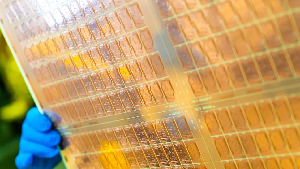
Glass wafer materials are emerging as a potential and viable alternative to their more conventional, aged organic counterparts. Replacing plastic-based cores with glass panels, these substrates offer lower warpage and a flatter overall profile, two properties that chipmakers will be keen to take advantage of as packaging becomes more of a performance limiter alongside silicon and memory.
Samsung, AMD, Intel, Broadcom, and even AWS have all been associated with glass-substrate evaluation as they contend with the challenges posed by growing package sizes and wiring density. Now, according to Korean supply chain reporting cited by DigiTimes, several Chinese companies from across PCBs, displays, and outsourced semiconductor assembly are understood to be moving into the glass substrate market as the technology is increasingly seen as “a new growth engine.”
Full-chain buildouts in China
Visionix, an advanced display solutions provider that spun out of Tsinghua University in 2001, and BOE Technology, one of the world’s largest manufacturers of OLED and flexible displays, were two of the most prominent companies named in the initial reporting, along with PCB supplier AKM Meadville and Yuntian Semiconductor.
According to industry sources, these companies are said to be involved in full-chain buildouts, with equipment and process capabilities assembled in parallel. Visionix alone is understood to have now begun “full-scale investment” after spending the second half of 2025 organizing a supply chain for materials and equipment. Meanwhile, BOE has already launched a glass substrate business following internal technical verification.
On the manufacturing side, AKM has built a pilot production line, while assembly and test giant Yuntian — which gained notoriety after entering Huawei’s supply chain — is also known to be assembling its own glass substrate capability. According to the industry sources cited by DigiTimes, Chinese suppliers are keen to move into this space quickly by standing up manufacturing flows all at once to shorten time to market, rather than scaling incrementally.
A pivot with risk
It should come as no surprise that capital scale and execution speed are being emphasized here. Chinese officials have been unusually transparent about the importance it is placing on establishing a domestic semiconductor market that can stand up to and compete with the West in the age of AI. It’s a matter of significant national importance to the Chinese, with Xi Jinping recently calling AI “epoch-making” and defining it as a core pillar of the country’s next five-year plan through 2030.
China’s approach here isn’t without risk. Glass substrates introduce entirely new defect modes and reliability challenges, and early missteps can be very expensive because these defects tend to appear later in the manufacturing process. Glass is, of course, brittle, so microscopic cracks from mishandling or drilling can survive early inspection and then propagate during thermal cycling or mechanical stress. It’s entirely possible — and arguably likely — that customers evaluating early glass-core packages will require extensive thermal cycling and long-term aging data before they can commit to volume production, potentially extending timelines beyond the 2027 to 2030 projections given by manufacturers currently working with the technology.
Chinese companies seem to be willing to absorb these challenges and the potential associated costs in exchange for a long-term competitive advantage in advanced packaging. And, at the same time, glass handling and high-throughput manufacturing are already core competencies of the likes of BOE and Visionix, who are uniquely positioned to redeploy their expertise into the semiconductor glass substrate market.
Racing towards first qualification
Outside China, companies in South Korea, Taiwan, Japan, and the U.S. are also exploring glass substrates. SK group subsidiary Absolics is among the most advanced and is expected to become the first company to commercialize the technology after beginning prototype production at its Georgia, U.S. facility last year. Meanwhile, Samsung Electro-Mechanics signed a memorandum of understanding with Sumitomo Chemical back in November to establish a joint venture for glass cores, while LG Innotek has delayed its glass substrate commercialization until 2030 due to demand uncertainty.
Naturally, companies linked to TSMC and major substrate suppliers like Unimicron are also exploring glass substrate options as part of their broader advanced packaging roadmaps, while Japan’s Dai Nippon Printing has been developing glass-core technology within its advanced packaging business. The company announced work on glass core substrates using high-density TGV aimed at next-gen semiconductor packages back in 2023, announcing the launch of a TGV glass core substrate pilot line at its Kuki Plant last December.
While all these companies are currently racing towards first qualification rather than full volume production, once a supplier manages to iron out defects and is qualified for flagship chip packaging, multi-year supply agreements will follow. It’s easy to see why China wants in on that, but ultimately, the pace at which Chinese suppliers can close any technical gaps will be the deciding factor on whether its entry to the market can shake up competition. A mature glass display sector may shorten the learning curve, but semiconductor packaging imposes punishingly tighter reliability and defect requirements than display manufacturing.

Follow Tom's Hardware on Google News, or add us as a preferred source, to get our latest news, analysis, & reviews in your feeds.

Luke James is a freelance writer and journalist. Although his background is in legal, he has a personal interest in all things tech, especially hardware and microelectronics, and anything regulatory.

