SK hynix to build first U.S. packaging plant for HBM — plugs critical hole in U.S. supply chain, $3.9B investment challenges TSMC and reshapes AI supply chains
Memory giant eyes turnkey HBM strategy with Indiana packaging line as U.S. reshoring effort accelerates.


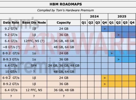
Want more? We've got an exclusive roadmap to the future of high-bandwidth memory — only for subscribers of Tom's Hardware Premium.
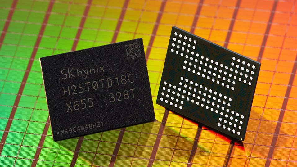
SK hynix is bringing its HBM ambitions to U.S. soil with a $3.9 billion plan to build its first domestic manufacturing facility — a 2.5D advanced packaging plant in West Lafayette, Indiana. The site, developed in partnership with Purdue University, is aimed at producing turnkey HBM modules for AI accelerators by 2028.
In bringing manufacturing to the U.S., SK hynix aims to vertically integrate its HBM supply chain, which currently relies on outside firms, to handle the delicate process of mounting HBM stacks to logic dies via interposers. That assembly work is increasingly a bottleneck for high-end GPUs, especially as demand for AI silicon continues to outstrip available packaging capacity. By owning both the memory and the interconnects, the company is clearly trying to target the kind of leverage that TSMC holds over the likes of Nvidia.
The Indiana facility, which is partially funded by $458 million in CHIPS Act grants and loans, is SK hynix’s first U.S. production site and part of a broader effort to bring critical semiconductor infrastructure closer to U.S. customers. It comes alongside the company’s new R&D outpost near Seattle, built in part to deepen ties with Nvidia and other domestic hyperscalers. When complete, the plant will package HBM chips with silicon interposers and integrate them with partner dies into a single, thermally optimized 2.5D module ready for use in AI servers or supercomputing clusters.
According to filings, SK hynix plans to operate a full mass-production line at the site, supported by a dedicated talent pipeline from Purdue. That puts it in direct competition with TSMC’s CoWoS platform, which has been the de facto standard for high-end HBM packaging since Nvidia’s Pascal era. And with TSMC’s CoWoS capacity effectively sold out through 2027, customers are already searching for alternatives.
Turnkey HBM
The biggest problem with HBM is that it’s a packaging challenge. HBM stacks multiple memory dies vertically using through-silicon vias (TSVs), all of which must be mounted on a large interposer next to a host processor. That assembly must account for thermal expansion, routing complexity, and thousands of microbumps, resulting in a tightly coupled chiplet module with massive I/O bandwidth and low power draw, ideal for AI training or HPC workloads.
Until now, HBM suppliers like SK hynix and Samsung have typically sold raw memory stacks, leaving GPU vendors to rely on foundry partners for packaging. Nvidia’s H100 and AMD’s MI300X, for instance, use HBM2e and HBM3 mounted via TSMC’s CoWoS process. But with demand for accelerators reaching historic highs — and HBM4 promising even more aggressive stack designs — the need for in-house packaging has become a priority.
SK hynix’s stated goal is to deliver a “turnkey” solution: HBM stacks already integrated with silicon interposers and, potentially, host dies from customers. That would allow hyperscalers or chip designers to skip TSMC entirely for final assembly, receiving ready-to-mount modules instead. It’s a fundamental shift in how HBM enters the supply chain, positioning SK hynix as a full-stack supplier rather than a component vendor.
This type of setup already has some precedent. TSMC has steadily expanded its role from foundry to integrator over the past decade, using its packaging platforms (CoWoS, InFO, SoIC) to create customer lock-in beyond wafer fabrication. SK hynix has obviously drawn inspiration from that playbook, starting from memory and working outward. It also places pressure on Samsung, which is reportedly evaluating its own U.S. packaging line to support future Tesla and AMD accelerator deployments.
The timing of all this is no accident. HBM demand is projected to be worth tens of billions by 2030, driven by AI model scaling and architectural shifts toward high-bandwidth chiplets. Nvidia’s Rubin platform — expected to launch late 2026 — will reportedly use HBM4E stacks with bandwidth over 1.2TB/s per module. That’s not achievable with standard memory interfaces or traditional DRAM. If SK hynix can offer a high-yield, pre-packaged solution at scale, it could become indispensable to Nvidia, AMD, and a whole host of other companies.
A national security priority
Advanced packaging has become a national security and industrial policy priority, and Washington is funding it accordingly. The Commerce Department’s CHIPS for America program set aside about $3 billion for the National Advanced Packaging Manufacturing Program to expand U.S. advanced packaging R&D and manufacturing capacity under the Biden administration in 2023, which remains under the incumbent Trump administration.
While TSMC and Intel have U.S. fabs in Arizona and Ohio, neither currently offers high-volume 2.5D packaging on U.S. soil. SK hynix's Indiana site will be the first to do so, and potentially the only one with dedicated capacity for third-party AI customers.
See, packaging isn't just about putting chips together; it determines yield, thermals, and even chip performance. Interposer routing, power distribution, and heat dissipation can make or break an accelerator, so by integrating packaging with memory production, SK hynix gains tighter control over thermal budgets and mechanical tolerances, reducing failure rates in multi-die modules. And by keeping the entire process in the U.S., it aligns with growing customer pressure to onshore AI supply chains.
TSMC is responding in kind, expediting its own Arizona-based packaging line with a target completion window of late 2027. But TSMC’s U.S. capacity is largely reserved for captive customers and its own Arizona wafer output. That leaves a vacuum for customers seeking independent packaging partners. SK hynix could fill that role, especially if its turnkey model proves more predictable than the fragmented flow of wafers and memory stacks across the Pacific.
This isn’t just about fabs versus packages, but rather, where the AI supply chain converges. The raw silicon may still come from Korea or Taiwan, but the modules that power large language models, scientific simulations, and autonomous workloads will increasingly be built where the compute is deployed. And if SK hynix succeeds, it won’t be the last memory maker to cross the packaging threshold.
Micron has already announced plans to co-locate HBM packaging at its Virginia site. Meanwhile, Samsung is in talks with U.S. partners, and Intel is integrating Foveros with its own internal chiplets. But with a turnkey HBM solution provided via a 2.5D packaging plant in the U.S., SK hynix could easily take the lead.
Follow Tom's Hardware on Google News, or add us as a preferred source, to get our latest news, analysis, & reviews in your feeds.


Luke James is a freelance writer and journalist. Although his background is in legal, he has a personal interest in all things tech, especially hardware and microelectronics, and anything regulatory.

