
Musk says Samsung's Texas fab outclasses TSMC's US-based fabs — with AI5 still in development, questions remain over whether Tesla will need advanced tools

Last week, Elon Musk announced that Tesla would make its next-generation AI5 processor in the U.S. and would double-source this system-on-chip from both TSMC and Samsung Foundry. This is down to Tesla aiming to have plenty of AI5 silicon available, since it will be used in a wide range of applications, including cars, robots, and, somewhat unusually, data centers. Musk also said that Samsung Foundry's fab in Taylor, Texas, is more advanced than TSMC's Fab 21 phase 1 in Arizona, which is a strange comment from a fabless chip designer.
We analyze what Samsung's Texas fab is capable of, how it compares to TSMC's fab 21 phase 1, and whether Musk's upcoming AI5 chip will really need the advanced capabilities that Samsung Foundry can offer.
More AI5 chips, more performance
Tesla's AI5 will be considerably more advanced than the AI4, according to Elon Musk. Since the company plans to use them broadly across its products, it wishes to maintain a surplus.
"I am confident [the AI5] will be winner, next level [of AI performance], so it makes sense to have both Samsung and TSMC focused on AI5," Musk said during an earnings call with investors and financial analysts this week.
Based on Musk's earlier comments, AI5 is a massive processor that can demand up to 800W (at peak). Without plenty of rudimentary IPs such as image signal processing or graphics processing, it leaves die space for low-precision tensor compute hardware to maximize performance and cost efficiency. Despite the high power consumption, the AI5 fits in 'a half reticle,' which equates to around 430mm^2, putting it in a happy middleground of not being too large, nor too small.
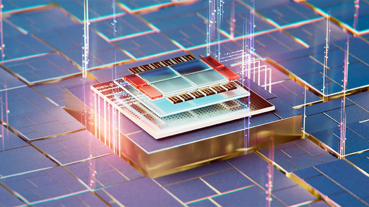
The exact configuration of Tesla's AI5 next-generation system-on-chip (assuming that it is a SoC, not a multi-chiplet SiP, or a series of products) is unknown; we only know it contains Arm CPU cores and plenty of proprietary Tesla hardware.
Due to this, it's difficult to ascertain just what lies under the hood of AI5, given its vast differences from AI4 in terms of power consumption (800W vs. 140W), lack of graphics processing and image processing capabilities, and the wide range of potential applications, which span from cars and robots to data centers.
"If we have too many AI5 chips for the cars and robots, we can always put them in the data center," Musk said. "So, we already use AI4 for training in our in our data center. So, [we] use a combination of AI4 and Nvidia hardware. So, we are not about to replace Nvidia, to be clear, but we do use both in combination, AI4 and Nvidia hardware. And the AI5 excess production, can always put in our data centers."
While Musk outlined vast volumes as one of the primary reasons behind the rather unusual decision of double sourcing a complex chip from two advanced foundries on two advanced nodes (which are yet to be determined), is perhaps another reason is to 'pipe clean' Samsung Foundry's American fab before assigning AI6 production exclusively (or maybe not exclusively) to SF, but Musk denied it.
Better equipment?
Musk also made an unusual comment regarding Samsung's Taylor, Texas fab tools, claiming that they are more advanced than TSMC's Fab 21 phase 1 in Arizona.
"Technically, the Samsung fab [in Texas] has slightly more advanced equipment than the TSMC fab [in Arizona]. These [AI5 chips] will be made in the U.S. […] by TSMC in Arizona, Samsung in Texas," Musk said.

Samsung's fab in Taylor, Texas, has been designed to produce chips on various manufacturing technologies, down to Samsung Foundry's SF2, which used to be called SF3P, but given its performance advantages over other SF3-series nodes, the company decided to bring it into the 2nm-class league. However, whether SF2 is competitive with Intel Foundry's 18A and TSMC's N2 remains to be seen, as other details, such as the number of EUV layers SF2 uses, are still a mystery.
While we do not know the exact configuration of Samsung Foundry's fab in Taylor, Texas, you can presume that it is tailored to make chips on 3nm-class process technologies, given its ramp timing in 2026 – 2027. So, we can expect Samsung to equip its fab for SF2P, SF2X, SF2A, and perhaps SF2Z (with backside power delivery), but this has not been officially confirmed.
Still, a fab capable of producing 3nm-class chips is indeed more advanced than TSMC's Fab 21 phase 1 in Arizona, which is designed to make chips on 5nm and 4nm-class production nodes. So, TSMC's fab 21 lags behind Samsung by design. Also, keep in mind that Samsung's leading-edge process technologies have relied on gate-all-around (GAA) transistors since SF3 in 2022, which require specialized tools to fabricate.
TSMC's Fab 21 phase 1 was designed and equipped between 2020 – 2024 (it likely follows TSMC's blueprints for its 1st-generation EUV-capable fabs). This is notably before ASML released its newer Twinscan NXE:3800E lithography systems, so the fab is equipped with Twinscan NXE:3600D machines, which can process up to 160 wafers per hour at a dose of 30 mJ/cm^2.
In contrast, Samsung Foundry's fab in Taylor is now being equipped, so if we were to speculate, we would imagine that Samsung equipped its fab in Taylor, Texas, with the more advanced Twinscan NXE:3800E, which processes up to 220 wafers per hour at 30 mJ/cm^2. Do bear in mind that ASML's scanners are upgradeable, so, theoretically, TSMC can boost the performance of the tools it uses if deemed necessary.

Because Samsung Foundry's fab in Taylor, Texas, is meant to produce chips relying on GAA transistors, it has more significant differences from TSMC's Fab 21 phase 1, which is designed to produce ICs with tried-and-true FinFET transistors.
GAA transistors introduce an entirely new level of complexity in both etching and deposition, because their architecture replaces a single vertical fin with multiple stacked horizontal nanosheets. Each sheet is separated by a temporary silicon-germanium (SiGe) layer that must be selectively etched away without damaging the adjacent silicon channels.
This requires atomic-layer etch (ALE) tools capable of removing material one or two angstroms at a time with extreme selectivity and directionality. These systems must also achieve near-perfect uniformity across 300mm wafers, since even slight over-etching can collapse or roughen the ultra-thin nanosheets. While TSMC hardly needs such tools at Fab 21 phase 1, Samsung does at its Taylor fab.
On the deposition front, conformal atomic-layer deposition (ALD) and selective epitaxy are key to device performance. The gate in a GAA device wraps fully around each nanosheet, requiring pinhole-free, uniform metal and dielectric films on all surfaces, even deep within narrow trenches. To produce them, chipmakers need tools that provide sub-angstrom control of high-k dielectrics (e.g., HfO₂) and metal gate layers (TiN, Ru, Mo) with near-perfect step coverage.
In addition, selective epitaxial deposition systems grow alternating Si/SiGe multilayers that form the nanosheet stack with atomic-scale thickness precision. Together, these advanced etch and deposition systems provide the precision and process stability necessary to manufacture GAA transistors reliably at the 3nm node and beyond. However, GAA transistors are not required for TSMC's N4 or N5 processes. TSMC is expected to debut GAA transistors in its 1.6nm-class 16A process.
Since the Samsung fab in Taylor, Texas, is at least one production node ahead of TSMC's Fab 21 phase 1, it features different metrology and inspection tools, too. Fab 21 phase 1 likely features a standard toolset from the late 2010s and early 2020s, so its in-line metrology/inspection stack is comprised of overlay/CD scatterometry, optical wafer inspection, and e-beam review tuned for 4nm and 5nm nodes. In contrast, Samsung's fab in Texas uses new generation tools, such as multi-angle scatterometry, X-ray, and e-beam or even multi e-beam metrology to ensure sub-angstrom control and uniformity across wafers.
But does Tesla AI5 need those advanced tools?
With the differences between the fabs out of the way, another question remains: Does Tesla's AI5 chip demand the advanced tools that Samsung Foundry's Taylor fab can provide? The simple answer is that we don't know, given the lack of specifics we have about AI5. The processor was expected to be released in early 2026, but then Tesla delayed it to late 2026. As Musk revealed last week, the hardware is still in development and has not taped out, so it is well over a year away from production.

"The AI5 chip designed by Tesla is, I think it is an amazing design, I have spent almost every weekend for the last few months with the chip design team working on AI5," said Musk. "I do not hand out praise easily, but I have to say that I think I think the Tensor chip team is really designing an incredible chip here. This is by some metrics, the AI5 chip will be 40 times better than the AI4 chip. Not 40%, 40 times. Because we have a detailed understanding of the entire software and hardware stack."
If Tesla tapes out AI5 this November, the earliest it can start mass production is December 2026. A more realistic timeframe is likely early 2027.
In any case, Samsung's Taylor fab is expected to start ramping up chip production sometime in 2026, so by late 2026 or early 2027, it will be ready for AI5. As for TSMC, the 3nm-capable Fab 21 phase 2 will only ramp in the second half of 2027. So, if Tesla plans to double-source AI5 from TSMC and Samsung Foundry starting in late 2026 or early 2027, it will likely rely on TSMC's N5A in Arizona and, presumably, the SF4A fabrication process in Texas.
In theory, Tesla could use SF2A, but we doubt it will be ready for large processors by early 2027, so SF4A is more likely, as it will be a mature automotive-grade fabrication technology by then. Furthermore, making the same chip on a 5nm-class process technology and Samsung's SF2 does not make much sense, as the final silicon will exhibit different power, thermal, and performance characteristics.
Faster production?
Given that Tesla's AI5 will almost certainly rely on FinFET transistors, it will make little use of the more advanced tools Samsung will have at its fab in Taylor, Texas, making Musk's comment largely irrelevant for the AI5 processor.
Perhaps, the main advantage of SF's fab for Tesla's AI5 is its Twinscan NXE:3800E lithography systems, which can process 40% more wafers per hour than their predecessors used at Fab 21 phase 1. This can potentially shrink cycle time and/or increase output. However, the actual cycle-time improvement across the entire fab is much smaller, as EUV exposure is only one part of a multi-hundred-step process.
Other tools, such as deposition, etch, inspection, and cleaning, dominate total wafer cycle time, which is around 12 weeks for 5nm-class products. So, at best, the newer ASML tools might cut total wafer cycle time by 5%–10%, but their performance advantage over predecessors will not translate into a 40% reduction in cycle time.
To sum things up, Musk's comment about Samsung Foundry's upcoming fab in Taylor, Texas, being 'more advanced' than TSMC's Fab 21 phase 1 is technically true, but it is largely irrelevant to Tesla's immediate production needs.

Follow Tom's Hardware on Google News, or add us as a preferred source, to get our latest news, analysis, & reviews in your feeds.
