
How TSMC managed to increase efficiency of ASML's EUV tools: System-level optimizations and in-house pellicles —chipmaker boosted EUV-driven wafer production by 30x over six years while reducing power consumption by 24%

TSMC is by far the largest operator of ASML's EUV lithography tools in the industry, with a second-to-none supply chain of both hardware and raw materials. The company's requirements for EUV pellicles (a thin membrane that protects the photomask, which acts as a stencil for chip patterns) have gotten incredibly high. The requirements are so extreme that TSMC intends to retrofit one of its 200-mm fabs to produce proprietary EUV pellicles exclusively, according to DigiTimes.
However, TSMC's proprietary pellicles, which outperform ASML's own offering, are just the tip of the iceberg, as TSMC pushes efforts to improve the efficiency of its fabs and ASML's EUV lithography tools.
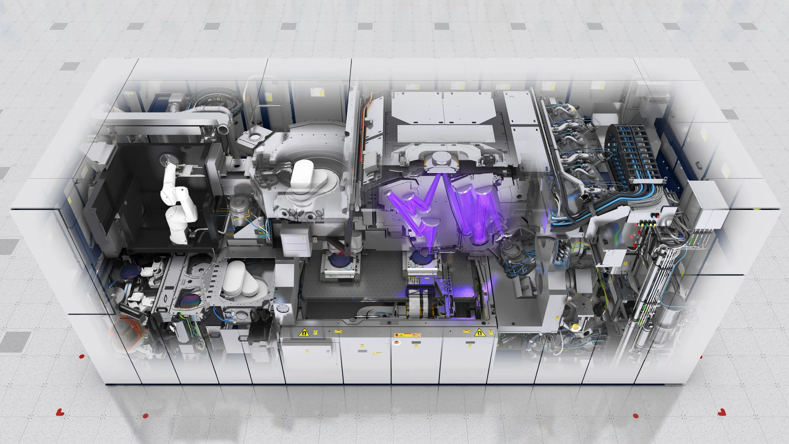
Tool productivity
TSMC said at its Technology Symposium in mid-2024 that it had doubled the wafer output per EUV tool per day since 2019 by fine-tuning both the exposure dose and the photoresist materials used in its lithography process. But, to define how TSMC has managed such efficiency, we speculate how the company may have achieved this.
On the exposure side, TSMC refined dose-to-size and dose-to-clear thresholds to reduce scanner dwell time per exposure field, while preserving critical dimension (CD) uniformity and ensuring line-edge roughness (LER) according to spec, which enables faster patterning without compromising yield in EUV lithography.
Typically, lowering these doses reduces the scanner's dwell time per field, enabling more wafers to be processed each day. However, this must be carefully balanced to maintain pattern fidelity, including CD control and LER. TSMC has succeeded, at least if we decoded its description correctly. Since TSMC has not disclosed the exact details, this is speculation, based on publicly available information.
On the materials side, TSMC upgraded its photoresist systems, possibly adopting high-sensitivity chemically amplified resists (CARs) and potentially incorporating metal-oxide resists (MORs) to improve absorption at 13.5 nm wavelength. These materials can enable lower exposure doses without degrading resolution. However, the company has yet to disclose which materials were used and exactly how they may have been implemented.
In parallel, TSMC also improved scanner utilization efficiency by deploying predictive maintenance models, optimizing job scheduling, servicing tools in advance, enhancing vibration control, and improving cooling performance. These changes reduced unplanned downtime and increased daily tool availability, enabling each EUV system to process more wafers in a stable environment.
Particular Pellicles
One of the most important advances has been in pellicle technology. These thin membranes protect EUV photomasks (reticles) from contamination, but have long been a bottleneck due to durability and defect issues. ASML itself developed two generations of its reticles, but it appears as though TSMC has managed to outpace them.

Back in mid-2024, TSMC reported dramatic improvements of its in-house developed EUV pellicle performance, including a four times longer lifespan, four and a half times more wafer output per pellicle, and an 80x reduction in defects. This likely points to TSMC's full-stack engineering approach that spans materials, mechanics, and fab integration.
On the materials side, TSMC may have adopted advanced pellicle films such as ultra-thin silicon-based membranes (e.g., SiNx, ZrSi2) or hybrid multilayers with optimized EUV transmittance, thermal stability, and mechanical strength. These materials withstand EUV radiation, minimize thermal deformation, and reduce outgassing. To further suppress particle adhesion and resist contamination-induced failures, TSMC likely treated the surface with anti-reflective coatings or plasma passivation; however, this is speculation and not officially confirmed.
There are additional ways to improve the lifespan of pellicles and reduce defects. For example, tighter cleanroom protocols would reduce the chance of particle transfer onto pellicles or reticles. However, TSMC has yet to disclose these methods.
Photomasks
In addition to pellicles that protect photomasks, TSMC is also refining the photomasks themselves. To meet the A14 node's lithography demands, TSMC improved mask accuracy and defect control to reduce defect density, boost yield, and ultimately increase throughput.

TSMC claims that its engineers had improved CD uniformity, pattern fidelity, and overlay precision for curvilinear features by modifying EUV mask blanks, increasing the resolution of multi-beam writers, and optimizing mask fabrication processes. These steps ensured a more consistent pattern transfer and better alignment across layers.
Defect control was a major focus, too. TSMC strengthened its pellicle inspection, reticle cleanliness, and developer rinse chemistry to suppress defects like bridging and pattern collapse. TSMC deployed advanced e-beam inspection techniques to detect sub-visible membrane defects and degradation early, enabling predictive maintenance and proactive replacement before catastrophic failures, which improves yields and lowers performance variability.
In the future, TSMC plans to develop next-generation blank materials and new process flows to support future EUV requirements.
Planarization
Improving photomasks and pellicles are not the only ways to lower defect density, increase yields, and reduce performance variability, particularly for 2nm and sub-2nm-class process technologies, according to TSMC. The company is working to improve polarization for its A16 and A14 fabrication processes.

Planarization is crucial in advanced EUV lithography because it ensures a uniformly flat wafer surface, which is critical for maintaining focus and pattern fidelity at sub-2nm nodes like TSMC's A16 and A14. EUV systems have an extremely shallow depth of focus, which is why any topographical variation could be a source of defocus, CD variation, or LER. Uneven surfaces also lead to non-uniform resist thickness, which affects dose absorption and etch uniformity. Also, overlay errors increase if subsequent layers are patterned on non-planar foundations.
TSMC likely improves this through advanced chemical mechanical planarization (CMP), optimizing slurry chemistry, pressure profiles, and endpoint detection to achieve tight within-wafer and wafer-to-wafer planarity control.
Energy efficiency
EUV scanners are known for heavy energy use, and here too TSMC has made progress. It says it reduced power consumption of EUV tools by 24% 'through innovative energy saving techniques.' The company's future target is a 1.5 times improvement in energy efficiency per wafer by 2030.

Reduction in EUV scanner power consumption was likely achieved through a combination of hardware-level and system-level optimizations, though which optimizations were made has not been disclosed. For example, TSMC could enhance the laser-to-EUV conversion efficiency, where a significant amount of energy is lost. Another key area is thermal management. TSMC likely refined liquid cooling systems, optimized coolant flow rates, and improved heat exchanger design to lower auxiliary power consumption while maintaining thermal stability.
On the system side of things, firmware and scheduler optimizations may have reduced idle-state energy use and improved synchronization between subsystems, reducing power draw during non-exposure operations. Predictive maintenance and better utilization analytics would help avoid performance degradation from inaccurate positioning, synchronization, or overheating, which prevents inefficient tool operation.
TSMC's position strengthens
Although TSMC was not the first chipmaker to adopt EUV lithography, it is currently the largest operator of EUV tools in the industry. Since 2019, the company has doubled wafer throughput per tool, reduced scanner power consumption by 24%, and achieved major gains in pellicle performance, including four times the lifespan and 80 times lower defects. To support these advancements, TSMC plans to retrofit a 200 mm fab to manufacture proprietary EUV pellicles that may surpass ASML's own. These efforts reflect TSMC’s broader strategy to control the full EUV stack—from materials to tool optimization.
Follow Tom's Hardware on Google News, or add us as a preferred source, to get our up-to-date news, analysis, and reviews in your feeds. Make sure to click the Follow button!
