TSMC gives an ultra-rare video look inside its fabs — 'Silver Highway' and fab tools revealed in flyby video of company's US Arizona Fab 21
A rare glimpse inside the fully operational N4/N5 cleanroom.

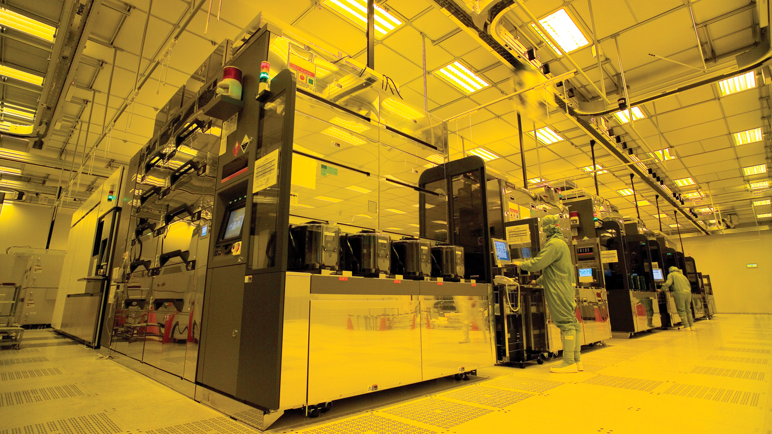
TSMC has published a flyby video over its Fab 21 near Phoenix, Arizona. The video shows hundreds of high-tech tools methodically crafting chips for various American companies. The crown jewels of the fab are of course ASML's Twinscan NXE extreme ultraviolet lithography tools that produce the most complex circuitry of such chips as Nvidia's Blackwell B300 processors.
I like how $TSM posted a video about its new Arizona Fab, where they explain how chips are made using EUV equipment from $ASML, and they even include small clips provided by $ASML."to be able to do this is incredibly difficult. We are using extreme ultraviolet technologies… pic.twitter.com/0iUqR13Z8JSeptember 7, 2025
Click 'See more' to see the embedded video.
This video provides an inside look at TSMC's Fab 21 phase 1 near Phoenix, Arizona, which is ramping up production of chips using N4 and N5 process technologies (4nm and 5nm-class). The video depicts a path over a cleanroom with yellow lighting that filters out shorter wavelengths to prevent unintended exposure of photoresists.
The opening sequence shows the so-called 'silver highway,' TSMC's automated material handling system (AMHS), consisting of overhead tracks transporting front-opening unified pods (FOUPs) carrying 300mm wafers. Hundreds of FOUPs are shown in motion to demonstrate meticulous logistics of wafers around the fab, something that is critical for maintaining cycle times in a high-volume manufacturing (HVM) environment.
Central to the video are ASML's EUV scanners (likely the Twiscan NXE:3600D), depicted 'printing' patterns on wafers in a Christopher Nolan's Oppenheimer-style video. EUV lithography uses CO2 13.5nm wavelength light generated via laser-produced plasma (LPP) from tin droplets, which are visible as purple plasma ignitions in chamber. LPP then hits the wafer, creating intricated pattens with resolutions down to ~13nm half-pitch in single-exposure for current nodes.
The video also highlights the challenges of EUV, such as overlay accuracy within a few nanometers (1.1nm for the NXE:3600D), stochastic effects, and the need for mirrors as traditional optics used in photolithography absorbs EUV lights. The video does not depict wafer stages and pellicles, which are customized by TSMC for extra performance, yet, we know that these critical components of EUV litho tools are of course present in the systems used at Fab 21 phase 1.
For now, TSMC is fabricating chips for companies like Apple, AMD, and Nvidia at its Fab 21 phase 1 using its N4 and N5 process technologies, but the company is also currently building its Fab 21 phase 2 that will be capable of producing chips on N3 and N2-series process technologies (something originally planned for Fab 21 phase 3), a long-rumored upgrade recently implied by the company's chief executive C.C. Wei.
Get Tom's Hardware's best news and in-depth reviews, straight to your inbox.
"We are preparing to upgrade our technologies faster to N2 and more advanced process technologies in Arizona, given the strong AI-related demand from our customers," Wei told analysts and investors last week. "Furthermore, we are close to securing a second large piece of land nearby to support our current expansion plans and provide more flexibility in response to the very strong multi-year AI-related demand. Our plan will enable TSMC to scale up to an independent Gigafab cluster in Arizona to support the needs of our leading-edge customers in smartphone, AI and HPC applications."
TSMC calls sites that have production capacities of over 100,000 wafer starts per month a 'Gigafab.'

Follow Tom's Hardware on Google News, or add us as a preferred source, to get our latest news, analysis, & reviews in your feeds.

Anton Shilov is a contributing writer at Tom’s Hardware. Over the past couple of decades, he has covered everything from CPUs and GPUs to supercomputers and from modern process technologies and latest fab tools to high-tech industry trends.
-
oskarkk Why link to a low quality fragment of the video reposted by random X user instead of linking to the full video from the official TSMC channel?Reply
eEsK-GJ9nBUView: https://www.youtube.com/watch?v=eEsK-GJ9nBU