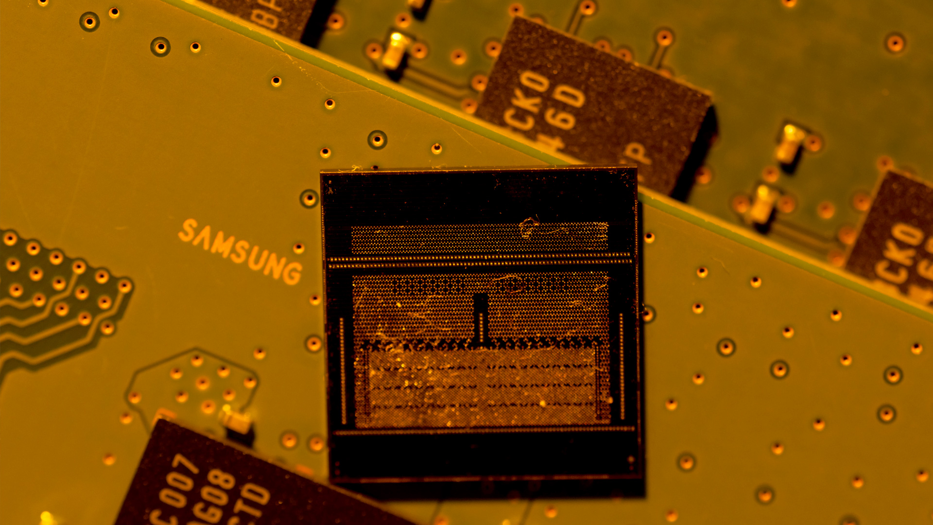
Samsung touts 96% lower-power NAND design — researchers investigate design based on ferroelectric transistors
Researchers demonstrate FeFET-based 3D NAND cells with near-zero pass voltage and up to five bits per cell.

Samsung researchers have published a detailed account of an experimental NAND architecture that aims to cut one of the technology’s largest power drains by as much as 96%.
The work — Ferroelectric transistor for low-power NAND flash memory — was carried out by researchers at the Samsung Advanced Institute of Technology and appears in the journal Nature. It describes a ferroelectric field-effect transistor (FeFET) design intended for future 3D NAND, combining a hafnia-based ferroelectric with an oxide-semiconductor channel and introducing a near-zero pass-voltage operation that forms the basis of the 96% power reduction figure.
In modern NAND, the stack of wordlines running through each vertical string must be biased with a pass voltage every time a cell is read or programmed. As layer count increases, so too does that overhead, and it now represents a significant share of total array power as a result of higher layer counts. The Samsung teams argue that a ferroelectric transistor with a wide memory window and a maximum threshold voltage pushed below zero can support multi-level operation without the high Vpass that charge-trap NAND relies on to avoid disturb.
They demonstrate this first in planar arrays operating at up to five bits per cell and then in a short four-layer vertical string designed to mimic 3D NAND geometry. The central gates in that structure measure 25 nanometres, similar to current commercial devices. The group defines a NAND-specific energy metric that combines the dominant contributions from wordline capacitance and the internal charge pumps that generate the high voltages required for reads and writes.
By modelling those costs for a full stack, the researchers estimate that a 286-layer device based on the ferroelectric design could reduce combined program and read energy by about 94% compared with a conventional charge-trap stack of the same height. At 1,024 layers, the reduction passes 96% as the lower pass voltage sharply lowers the work done by the charge pumps.
The experiments also cover retention and cycling limits. In planar form, the ferroelectric cells support a wide memory window and demonstrate five-level programming, although endurance at that density is modest. A PLC-class configuration holds for a few hundred cycles, while QLC-equivalent use approaches a thousand at both room temperature and 85 °C. The authors note that further development of program-inhibit schemes and negative-voltage generation will be required before a full 3D array could be qualified for production. They also point out that the oxide channel’s behaviour under high-temperature stress remains a key area for follow-up work.
As of now, there is nothing to suggest that Samsung plans any product announcements based on this work. Instead, the study is being framed as a piece of foundational research, which itself requires further development, for potential low-power NAND generations beyond the current charge-trap roadmap.
Get Tom's Hardware's best news and in-depth reviews, straight to your inbox.

Follow Tom's Hardware on Google News, or add us as a preferred source, to get our latest news, analysis, & reviews in your feeds.

Luke James is a freelance writer and journalist. Although his background is in legal, he has a personal interest in all things tech, especially hardware and microelectronics, and anything regulatory.
-
Stomx NAND companies feeding us with the tales on their great future QLC, PLC and so on while absolutely all current consumer grade NAND TLC have endurance less than 600. Stop making and selling crap to the masses which only works when you are an obtuse technophobeReply