Chinese researchers hail breakthrough in DRAM-like cells, which could be used in embedded or 3D stacked memory — absence of manufacturing detail casts doubt on mass production
Uncertainties make it impossible to evaluate commercial viability

Get Tom's Hardware's best news and in-depth reviews, straight to your inbox.
You are now subscribed
Your newsletter sign-up was successful
Chinese researchers have developed a capacitor-less DRAM-like memory cell that uses two transistors (2T0C) with dual-gate control, built at a 4F² minimum area, reports TrendForce, citing ResearchGate. The new memory cell architecture uses a self-aligned process. It promises to achieve reliable multi-bit storage, fast DRAM-like write times, and extended retention without a discrete storage capacitor, according to its developers. While it's not a DRAM replacement for now, it could become a viable solution for various eDRAM and stacked 3D memory applications.
Sanctions imposed by the U.S. and its allies on China's semiconductor sector greatly limit the capabilities of the People's Republic to produce chips on advanced production nodes, as companies like CXMT, SMIC, and YMTC do not have access to the latest tools. However, curbing pathfinding, research, and development (R&D) in academia is considerably harder (if possible at all), which is why Chinese scientists can conduct world-class research and develop innovative technologies that are on par with the West.
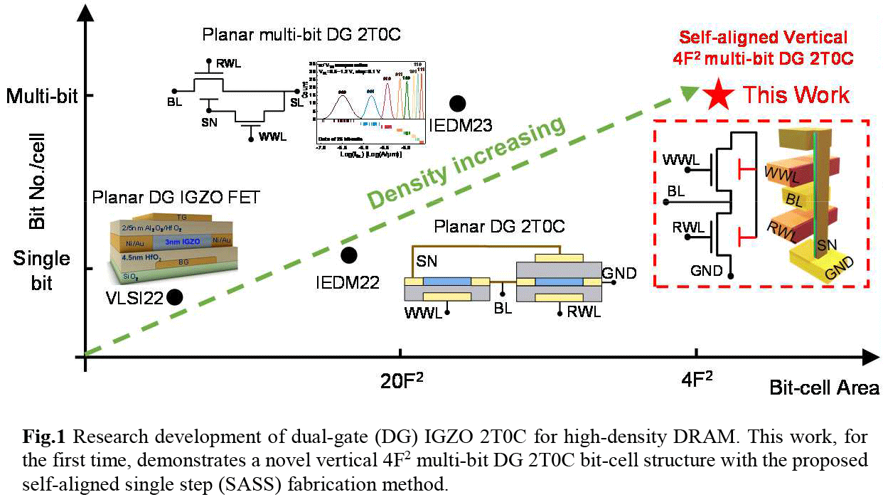
Before we proceed, let's establish some terminology to avoid confusion. In semiconductor memory discussions, 4F², dual-gate 4F², and 4F² 2T0C are often used interchangeably, even though they describe different layers of the design stack. While all three can appear in the same sentence, each answers a fundamentally different question: how dense the cell is, how the transistor is built, and how the bit is stored.
Article continues below 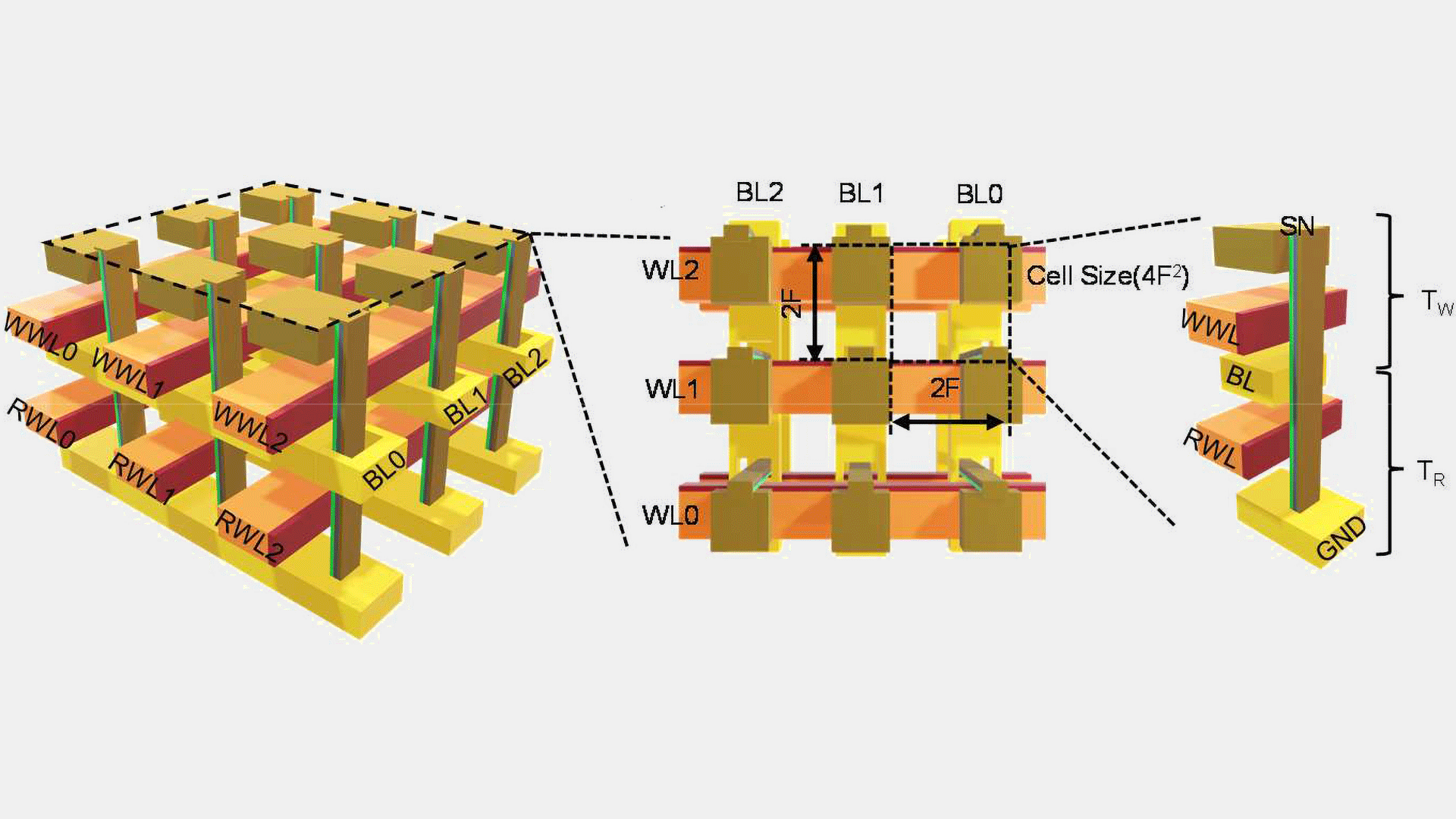
- 4F² is a layout and density metric that defines the minimum possible area of a memory cell — four times the square of the process feature size — and says nothing about the internal structure of the cell. A 4F² footprint can host a classic 1T1C DRAM cell, an SRAM bitcell, or even a resistive memory element.
- The term 'dual-gate' describes a device-level detail: a dual-gate transistor uses two independently controlled gates to improve electrical control over the channel, reduce leakage, and stabilize threshold voltage. Dual-gate transistors are widely used in the semiconductor industry in logic (FinFET is a dual-gate transistor), SRAM, or DRAM-like cells.
- Finally, 4F² 2T0C describes the actual memory architecture featuring two transistors that store data without a dedicated capacitor by relying instead on charge retained in a transistor channel or floating node. This design gives the cell DRAM-like behavior: it still needs refresh, but avoids the scaling challenges associated with deep capacitors.
When combined, the phrase 'dual-gate 4F² 2T0C memory' means a capacitor-less DRAM cell, based on dual-gate transistors, with DRAM-class density at a minimum. In short, we are dealing with three separate concepts combined in a unique design, rather than a singular invention.
4F² dual-gate 2T0C memory
Being unconstrained by curbs set by the U.S. and allies, National Key Laboratory of Integrated Circuit Manufacturing Technology at the Institute of Microelectronics of Chinese Academy of Sciences (IME CAS) teamed up with the Beijing Superstring Academy of Memory Technology (SAMT), and Shandong University to develop a 4F² 2T0C memory cell architecture that can store two bits of data per-cell (4 levels of charge), offering a write latency of around 50ns, and data retention for up to 470 seconds, making it a viable memory technology. However, while this isn't a DRAM killer, it may be a potent candidate for embedded DRAM and stacked 3D memory built on top of logic.
The breakthrough
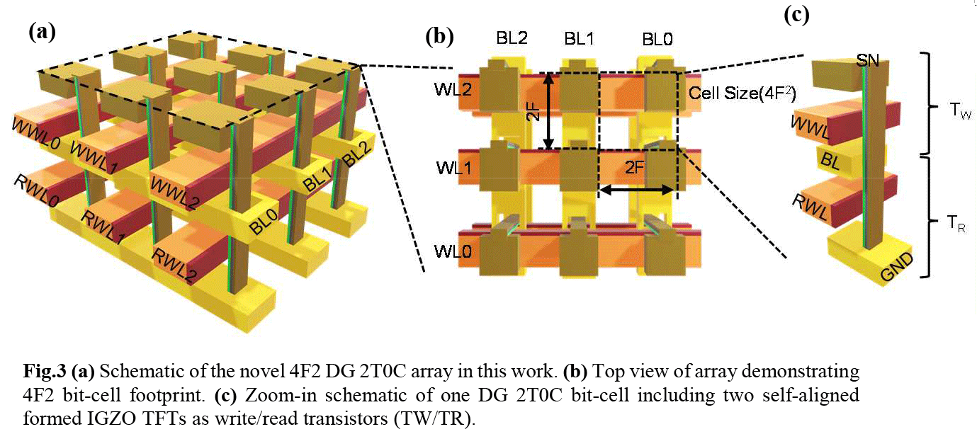
The 4F² dual-gate 2T0C memory cell architecture developed by researchers at IME CAS uses two vertical IGZO transistors—one for write (TW) and one for read (TR)—that share a common storage node (SN). Dual-gate operation improves electrostatic control and read stability, enabling capacitor-less, multi-bit storage (2 bits demonstrated) within a compact 4F² footprint. The scientists used a self-aligned single-step (SASS) process to build the cell.
Tests conducted by IME CAS scientists prove that the vertical dual-gate transistor combines high drive current with a sharp turn-on, which makes it easier to clearly distinguish stored charge levels during reads. The cell can hold data for about 470–500 seconds for '1' and '0,' respectively, which is inherently higher than that of DDR5 (which counts in milliseconds), but it is certainly not enough for a storage device.
In addition, the cell can complete a write operation in roughly 50ns, according to its developers. While a 50ns latency is comparable to that of DDR5 (which is about 20 – 40ns), read latency is much more important for real-world performance, but since it depends on sense amplifier architecture (keep in mind that we are dealing with multi-bit storage here) and the actual system, scientists from IME CAS do not publish it.
Reliability testing at 85°C confirms that the device remains stable under prolonged thermal and electrical stress, and threshold voltage shifts are limited to −22.6 mV under negative bias temperature stress (NBTS) and 87.7 mV under positive bias temperature stress (PBTS). A threshold-voltage shift below about 100 mV is considered functionally benign because it does not materially change the transistor’s on/off behavior, timing, or noise margins, so seeing <100 mV shifts at 85°C under accelerated stress can be considered as strong stability (especially for IGZO transistors that are vulnerable to bias stress).
The magic behind the reliable operation of the 2-bit 4F² dual-gate 2T0C memory cell, as well as its solid retention time, is the usage of both gates of the read and write transistors as capacitive contributors to the same storage node, which doubles storage node capacitance (CSN) compared to single-gate cells, without increasing overall area. As a result, the 2-bit 4F² dual-gate 2T0C memory cell architecture can enable both high density and high reliability at a small area.
SASS production flow
Scientists at IME CAS used its proprietary self-aligned single-step (SASS) production flow to build their 4F² dual-gate 2T0C memory cell. The SASS flow enables the entire vertical dual-gate 2T0C sidewall stack to be built in just one lithography and etch step that simultaneously patterns all pre-deposited layers. This means that write (TW) and read (TR) transistors are formed simultaneously rather than stacked in separate passes, which excludes misalignment and repeated thermal/contamination exposure, which potentially improves yields.
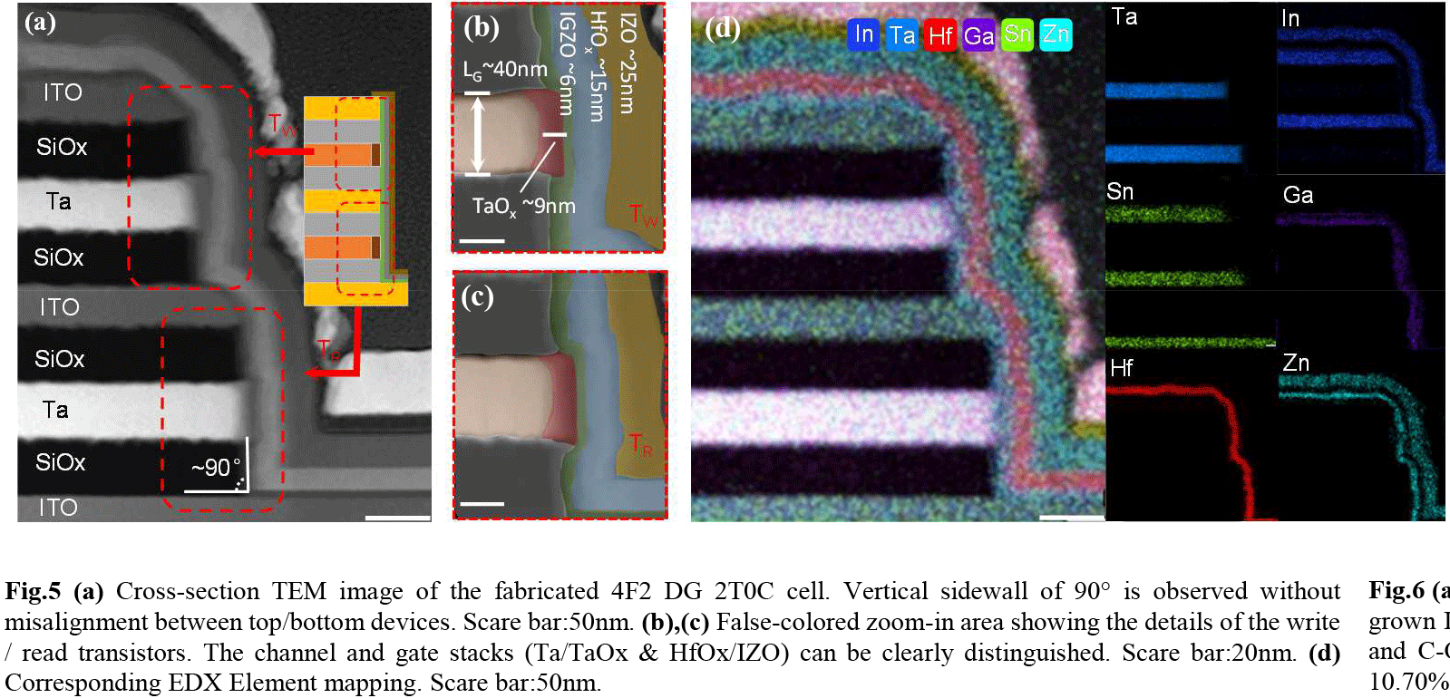
In the demonstrated 4F² vertical cell, the channel height is 120nm, the IGZO channel thickness is ~6nm (it is deposited using atomic layer deposition), and the effective gate length is ~40 nm, as seen in the cross-sectional TEM image. The TEM image also confirms a ~90° vertical sidewall with no top/bottom-device misalignment.
As noted above, the SASS process produces the full stack in one lithography/etch step that patterns pre-deposited layers, which is a fairly simplistic manufacturing method.
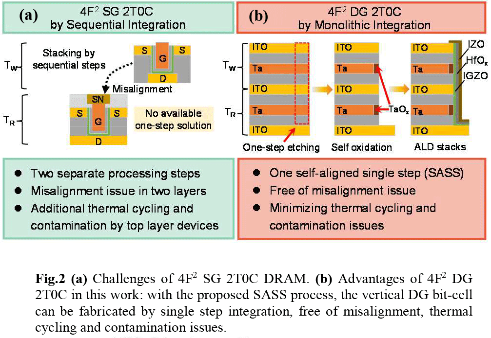
First, the researchers deposit a full multilayer stack on the wafer. This stack already includes everything the cell will need later: 30nm of indium tin oxide for ground (GND), the bit line (BL), and the storage node (SN); 40nm of tantalum for the read and write word lines (RWL/WWL); and 40 nm layers of silicon oxide to electrically isolate them. Altogether, the structure consists of five electrode layers separated by four SiOx layers, all deposited before any patterning takes place.
Next comes the main SASS step. Using one lithography mask and one vertical etch, the process cuts through the entire pre-deposited stack at once. This single etch step patterns all five electrode layers and four insulating layers at the same time into a clean vertical sidewall. Since everything is defined in one cut, the write and read transistors are perfectly aligned by design: there are no overlay errors from multiple patterning steps, which is why it is called 'self-aligned.'
Once the sidewall is in place, it is turned into an active device. The exposed tantalum is heated in oxygen at 400 °C, where it self-oxidizes to form a ~9 nm tantalum-oxide high-k gate dielectric directly on the metal. The vertical surface is then coated layer by layer: a ~6 nm IGZO channel is deposited using ALD, followed by the second gate stack, made up of a ~15 nm hafnium-oxide dielectric and a ~25 nm indium-zinc-oxide conductive gate layer.
But is it viable?
Despite detailed knowledge of device-level and vertical nanometer-scale dimensions, the absence of disclosed lateral half-pitch information prevents mapping the IME CAS process to a specific DRAM node. Keeping in mind that we are dealing with a research-grade materials stack and have no idea about yields, any general assessment of the cost efficiency of the process would be inaccurate.
That said, while the production flow looks simple and the lack of capacitors opens doors for eDRAM applications (as logic nodes are not exactly great for producing DRAM-class capacitors), there are questions about the practicality of 4F² dual-gate 2T0C memory. First up, a multi-level cell architecture requires advanced sense amplifiers that are both complex and power hungry, something not appreciated by embedded applications. Secondly, while IGZO TFTs are mature in displays as feature sizes are fairly large and yields are high (and forgiving), memory arrays demand dramatically smaller sizes, and defects are not forgiving.
Given all the uncertainties, it is impossible to assess whether IME CAS's 4F² dual-gate 2T0C memory architecture makes sense for commercial applications.
Despite similarieis, it's not a replacement for DRAM
Chinese researchers from IME CAS have demonstrated a 4F² dual-gate 2T0C, capacitor-less DRAM-like memory cell that reaches the minimum DRAM-class cell area without using a storage capacitor.
The cell is fabricated using a self-aligned single-step (SASS) process and is based on two vertical IGZO transistors sharing a common storage node. Tests conducted by IME CAS show 2-bit storage per cell, write times of around 50ns, and data retention of roughly 470–500 seconds, while the devices remain stable at 85°C. Meanwhile, the dual-gate design enhances retention by increasing the effective storage-node capacitance without increasing the cell area.
For now, 4F² dual-gate 2T0C DRAM-like memory is not a replacement for commodity DRAM. Yet, the work points to a route for embedded and 3D-stacked memory. However, the absence of disclosed lateral pitch, information about manufacturability, the multi-level cell architecture, and uncertainties about the feasibility of IGZO TFTs for mass production of memory cast doubt about the future of this memory architecture. But although we can question the practical applicability of 4F² dual-gate 2T0C DRAM-like memory architecture for existing applications and products, this does not belittle the achievement of Chinese scientists, who managed to make this technology work.

Anton Shilov is a contributing writer at Tom’s Hardware. Over the past couple of decades, he has covered everything from CPUs and GPUs to supercomputers and from modern process technologies and latest fab tools to high-tech industry trends.

