Nvidia enterprise GPU and CPU roadmaps: Rubin, Rubin Ultra, Feynman, and silicon photonics
Systems are planned to be up to 14 times faster than NVL72 by 2027.
Get Tom's Hardware's best news and in-depth reviews, straight to your inbox.
You are now subscribed
Your newsletter sign-up was successful
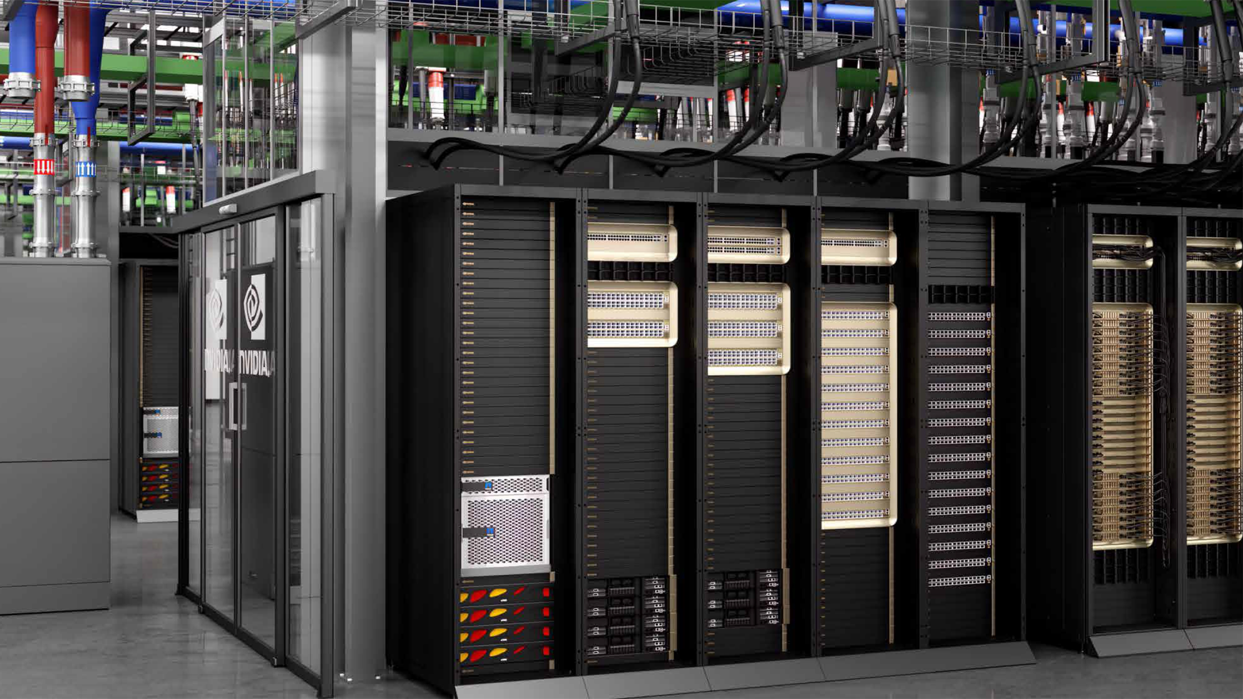
Nvidia recently disclosed plans for the next three years at GTC 2025, unveiling several generations of its GPUs, CPUs, networking gear, and systems. For Nvidia, displaying a comprehensive roadmap that clearly shows the evolution of its hardware is as important as executing it: Data center customers in particular need to understand where the company is going with its products and what to expect from its next-generation processors.
Nvidia has already lifted the lid on plans for Rubin GPUs, Vera CPUs, Feynman GPUs, and many other products that it plans to release over the next three to four years. Here's what it all means.

GPU roadmap
Nvidia is currently shipping its B200 and GB200 platforms based on the Blackwell architecture, and at GTC 2025, the company introduced its successor, Blackwell Ultra, which will be officially branded as the B300-series GPUs.
Article continues belowYear | 2022 | 2023 | 2024 | 2025 | 2026 | 2027 |
|---|---|---|---|---|---|---|
Architecture | Hopper | Hopper | Blackwell | Blackwell Ultra | Rubin | Rubin |
GPU | H100 | H200 | B200 | B300 (Ultra) | VR200 | VR300 (Ultra) |
Process Technology | 4N | 4N | 4NP | 4NP | N3P (3NP?) | N3P (3NP?) |
Physical Configuration | 1 x Reticle Sized GPU | 1 x Reticle Sized GPU | 2 x Reticle Sized GPUs | 2 x Reticle Sized GPUs | 2 x Reticle Sized GPUs, 2x I/O chiplets | 4 x Reticle Sized GPUs, 2x I/O chiplets |
Packaging | CoWoS-S | CoWoS-S | CoWoS-L | CoWoS-L | CoWoS-L | CoWoS-L |
FP4 PFLOPs (per Package) | - | - | 10 | 15 | 50 | 100 |
FP8/INT6 PFLOPs (per Package) | 2 | 2 | 5 | 5 | ? | ? |
INT8 POPS (per Package) | 2 | 2 | 5 | 0.330 | ? | ? |
BF16 PFLOPs (per Package) | 0.99 | 0.99 | 2.5 | 2.5 | ? | ? |
TF32 PFLOPs (per Package) | 0.495 | 0.495 | 1.15 | 1.25 | ? | ? |
FP32 PFLOPs (per Package) | 67 | 67 | 0.08 | 0.08 | ? | ? |
FP64/FP64 Tensor TFLOPs (per Package) | 34/67 | 34/67 | 40 | 1.3 | ? | ? |
Memory | 80 GB HBM3 | 141 GB HBM3E | 192 GB HBM3E | 288 GB HBM3E | 288 GB HBM4 | 1 TB HBM4E |
Memory Bandwidth | 3.35 TB/s | 8 TB/s | 8 TB/s | 4 TB/s | 13 TB/s | 32 TB/s |
HBM Stacks | 5 | 8 | 8 | 8 | 8 | 16 |
NVLink | NVLink 4.0, 50 GT/s | NVLink 4.0, 50 GT/s | NVLink 5.0, 200 GT/s | NVLink 5.0, 200 GT/s | NVLink 6.0 | NVLink 7.0 |
SerDes speed (Gb/s unidirectional) | 112G | 112G | 224G | 224G | 224G | 224G |
GPU TDP | 700 W | 700 W | 1200 W | 1400 W | 1800 W | 3600 W |
CPU | 72-core Grace | 72-core Grace | 72-core Grace | 72-core Grace | 88-core Vera | 88-core Vera |
The name Blackwell Ultra (2025) implies an increased performance variant of the B300 GPU over the B200 processors. But its performance increases do not come from higher clocks or optimized silicon.
While Nvidia claims the B300 GPUs offer 50% higher FP4 performance compared to their B200 counterparts (15 PFLOPs vs. 10 PFLOPS), the performance improvement comes with significant trade-offs.
The B300 has dramatically lower INT8, and FP64 performance compared to the B200. This makes it unsuitable for traditional supercomputers. So, if Nvidia plans to address this market going forward using Blackwell, it will have to keep offering B200 GPUs alongside its newer B300 GPUs in 2025–2026.
Nvidia’s B300 processors will retain the dual-chiplet design with the CoWoS-L packaging used in B200, and will continue to feature four HBM3E stacks per GPU chiplet. Initially, Nvidia plans to offer B300 with 288 GB of HBM3E memory, but eventually, the company could adopt 12-Hi HBM3E stacks and increase memory capacity.*
*Note: This is a potential development based on media reports, rather than an officially confirmed plan.
Nvidia’s next-generation architecture for data center GPUs is named after Vera Rubin (2026), an astronomer. This will be the first iteration of Rubin processors for data centers — let’s call them VR200 for now, assuming Nvidia will continue its conventional naming scheme.
VR200 will feature two reticle-sized GPU chiplets made on TSMC’s 3nm-class (Potentially N3P) fabrication process, two I/O chiplets, and 288 GB of HBM4 memory in eight stacks, with a data transfer rate of 6.40 GT/s, which will reach a peak bandwidth of around 13 TB/s.
The company’s Rubin GPUs will again double down on performance for AI applications, so their FP4 performance will increase to 50 PFLOPS in inference workloads, and to around 17 INT8 PFLOPS for training workloads. As of the time of writing, Nvidia has not disclosed the performance of VR200 GPUs with other data formats, though it is reasonable to expect tangible performance increases over Blackwell.
That performance increase will come with significantly higher power consumption. For now, Nvidia points to 1,800 W per GPU, which will increase the power supply requirements of data centers.
With the Hopper and Blackwell generations, refreshed GPUs offered tangible but not revolutionary performance upgrades. With the Rubin generation, the VR300 Rubin Ultra (2027) GPU promises to offer twice the performance of the VR200, as the refreshed GPU will use four GPU chiplets instead of two, and will therefore deliver 100 PFLOPS of FP4 performance for inference workloads.
Furthermore, the VR300 GPU will also support 1024 GB (1 TB) of HBM4E memory per package, with 32 TB/s of bandwidth. This will demand 3,600W of power per package and will therefore require extreme cooling methods. For those who need maximum performance density and have data centers that can accommodate machines with such GPUs, Rubin Ultra may be a solution.
The cost of Rubin Ultra is something we can only wonder about, of course. Nvidia will use TSMC’s CoWoS-L packaging for both Rubin and Rubin Ultra GPUs. In the case of the latter, it will need to integrate four near-reticle-sized GPUs, with two I/O dies alongside 16 HBM4E memory stacks.
Based on the image provided by Nvidia, it appears they are not using vertical stacking here, so either the company will use TSMC’s innovative 9.5-reticle-sized CoWoS-L interposer solution with a 120×150 mm substrate (which is expected to be ready in 2027, in time for Rubin Ultra), or it will stitch together two CoWoS-L interposers of smaller sizes.
Nvidia’s GPU roadmap continues in 2028 with the codenamed Feynman GPUs, and Nvidia has disclosed little about these processors for now. However, a surprising part is that it is said to use “next-generation HBM” memory in 2028. It is unclear whether Nvidia means a customized version of HBM4E tailored for AI and/or HPC workloads, or HBM5. And we certainly do not expect HBM5 to arrive this early.
CPU roadmap
In addition to GPUs, Nvidia offers Arm-based data center-grade CPUs with its systems.
Both Blackwell GB200 and Blackwell Ultra GB300 systems will keep using Grace CPUs with 72 Arm Neoverse V2 cores. The company’s CPU cadence seems to be one processor generation every two GPU generations, so Nvidia offers Grace both with Hopper and Blackwell processors.
The company plans to roll out its Vera CPUs alongside its Rubin GPUs in 2026, which will be used for Rubin and Feynman-based systems. Vera CPUs will pack 88 fully-custom Arm cores with Simultaneous Multi Threading (SMT), and will feature a 1.8 TB/s NVLink-C2C (900 GB/s in both directions) interface to connect to Rubin, Rubin Ultra, and Feynman GPUs.
NVLink roadmap
While it is crucial for Nvidia to deliver the fastest GPUs for AI and HPC on the planet, it is also crucial for the company to enable scale-up capabilities of its processors. That makes the evolution of low-latency, high-bandwidth connections imperative for Nvidia.
NVLink allows for chip-to-chip interconnection technology for both CPU-to-GPU and GPU-to-GPU connections. Nvidia also offers NVSwitch, which is used to connect GPUs within one rack (such as NVL72).
Nvidia’s current-generation Blackwell processors rely on the company’s 5th Generation NVLink technology with a 100 GT/s data transfer rate and PAM4 signaling, with a per-GPU bandwidth of 1.8 TB/s (900 GB/s in each direction, using 18 links or 36 lanes).
Each NVSwitch 5 chip features 144 NVLink ports (connecting 72 dual-chiplet B200 GPUs), each capable of 100 GB/s bidirectional bandwidth, totaling 14.4 TB/s per switch. This enables the 72 dual-chiplet B200 GPUs to ‘talk’ to each other concurrently at full speed, which allows the whole system to work like one large GPU.
With Rubin (2026), Nvidia plans to increase NVLink 6.0 bandwidth to 3.6 TB/s (1.8 TB/s in each direction). However, it is unclear whether the intention is to increase the data transfer rate or the number of lanes per link. In any case, with an NVSwitch 6.0, Nvidia’s NVL144 machine (with 72 dual-chiplet GPUs) will feature an NVLink bandwidth of around 28.8 TB/s, enabling significantly higher performance.
With Rubin Ultra (2027), Nvidia intends to transition to NVLink 7.0 and NVSwitch 7.0, but it will retain the NVLink bidirectional bandwidth at 3.6 TB/s, which likely means an increase in the number of ports-per-switch to 144, which will enable connection of quad-chiplet Rubin Ultra GPUs.
Networking roadmap
Internally, Nvidia GPUs within a DGX or NVL72 system are interconnected with NVLink and NVSwitch for extremely efficient intra-node performance. However, externally, multiple systems are interconnected via InfiniBand or high-speed Ethernet for large-scale AI workloads, enabling systems like Nvidia’s DGX SuperPOD.

With Blackwell-based machines, Nvidia uses Spectrum-5 Ethernet switches, and BlueField-3 SuperNIC, or a ConnectX-8 InfiniBand SuperNIC, which achieves up to 800 Gb/s network speed.
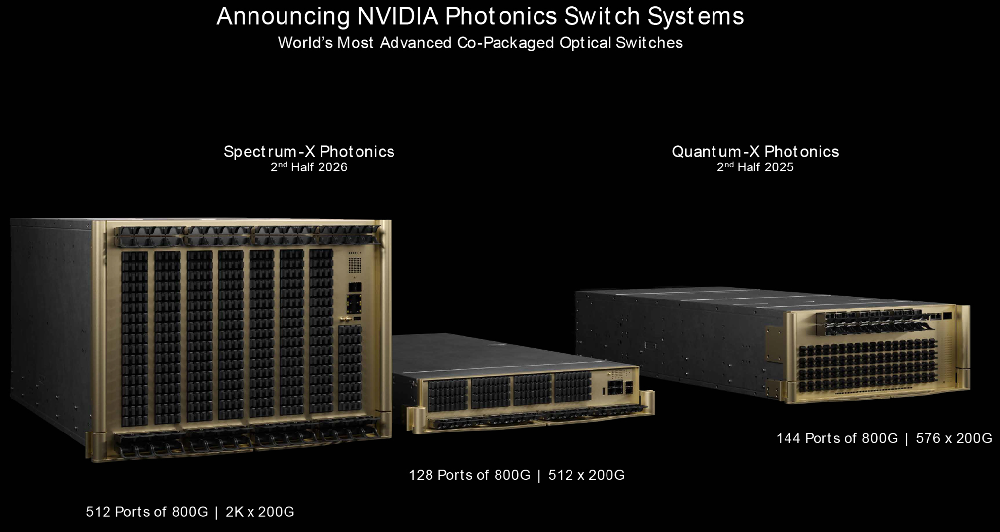
But, as GPUs become more powerful and bandwidth-hungry, and customers need clusters with more GPUs, Nvidia will need to adopt faster networking technologies. So, starting from the Rubin (2026) GPU generation, it will switch to Spectrum-9 Photonics and Quantum-X Photonics networking switch platforms to achieve exascale data centers.
Nvidia’s Spectrum-6 Photonics Ethernet and Quantum-CX9 Photonics InfiniBand platforms. Both are based on TSMC’s COUPE technology, which integrates a 65nm electronic integrated circuit (EIC) with a photonic integrated circuit (PIC). This is set to deliver 1.6 Tb/s per port — twice the bandwidth of leading copper Ethernet solutions — and will reach a total bandwidth of up to 400 Tb/s, through various high-density configurations.
Spectrum-X will be available in setups with 128 ports at 800 Gb/s or 512 ports at 200 Gb/s, both providing 100 Tb/s total throughput. A higher-capacity Spectrum-X model scales further, offering either 512 ports at 800 Gb/s or 2,048 ports at 200 Gb/s, achieving a maximum bandwidth of 400 Tb/s. The Quantum-X Photonics InfiniBand switch will feature 144 ports at 800 Gb/s or 576 ports at 200 Gb/s.
With Feynman (2028) GPUs, Nvidia’s data center platforms will transition to an 8th Generation NVSwitch, as well as next-generation Spectrum 7 Ethernet, and CX10 InfiniBand optical interconnects with increased performance. However, Nvidia has not disclosed any performance numbers for any of these parts quite yet.
System roadmap
In addition to offering advanced GPUs for AI and HPC, Nvidia is set to continue promoting its full-stack AI approach, integrating compute (CPU and GPU), networking, and software solutions to enable simplified AI deployment across various industries.
Year | 2022 | 2023 | 2024 | 2025 | 2026 | 2027 |
|---|---|---|---|---|---|---|
Density | NVL8 | NVL8 | NVL72 | NVL72 | NVL144 | NVL576 |
GPU Architecture | Hopper | Hopper | Blackwell | Blackwell Ultra | Rubin | Rubin |
GPU/GPU+CPU | H100 | H200 | GB200 | GB300 | VR200 | VR300 |
Compute Chiplets | 8 | 8 | 144 | 144 | 144 | 576 |
GPU Packages | 8 | 8 | 72 | 72 | 72 | 144 |
FP4 PFLOPs (Dense) | - | - | 720 | 1080 | 3600 | 14400 |
HBM Capacity | 0.6 TB | 1.1 TB | 14 TB | 21 TB | 21 TB | 147 TB |
HBM Bandwidth | 27 TB/s | 38 TB/s | 576 TB/s | 576 TB/s | 936 TB/s | 4,608 TB/s |
CPU | 72-core Grace | 72-core Grace | 72-core Grace | 72-core Grace | 88-core Vera | 88-core Vera |
NVSwitch | NVSwitch 3.0 | NVSwitch 3.0 | NVSwitch 5.0 | NVSwitch 5.0 | NVSwitch 6.0 | NVSwitch 7.0 |
NVSwitch Bandwidth | 1600 GB/s | 1600 GB/s | 3600 GB/s | 3600 GB/s | 7200 GB/s | 14400 GB/s |
Scale-Out | 400G/800G, copper | 400G/800G, copper | 800G, copper | 800G, copper | 1600G, optics | 1600G, optics |
Form-Factor Name | HGX | HGX | Oberon | Oberon | Oberon | Kyber |
With Blackwell, Nvidia intends to focus on its NVL72 ‘Oberon’ liquid-cooled system design, packing 72 dual-chiplet GB200 and GB300 GPUs.
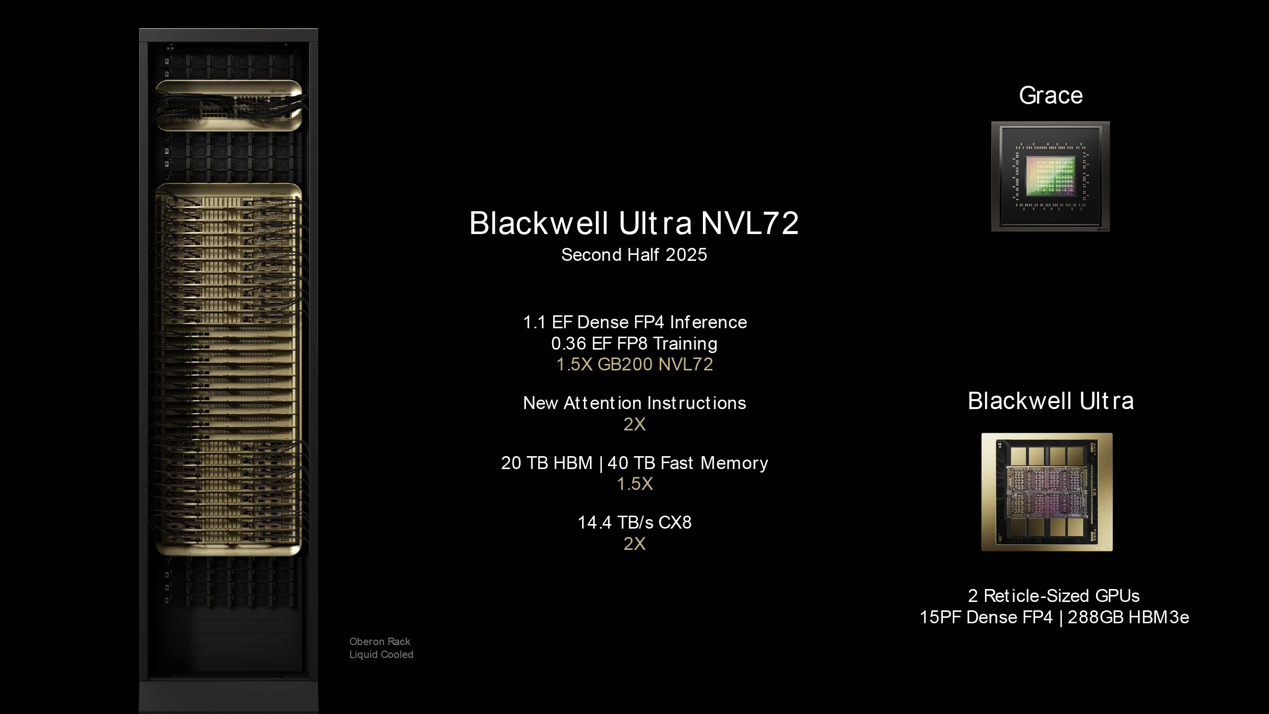
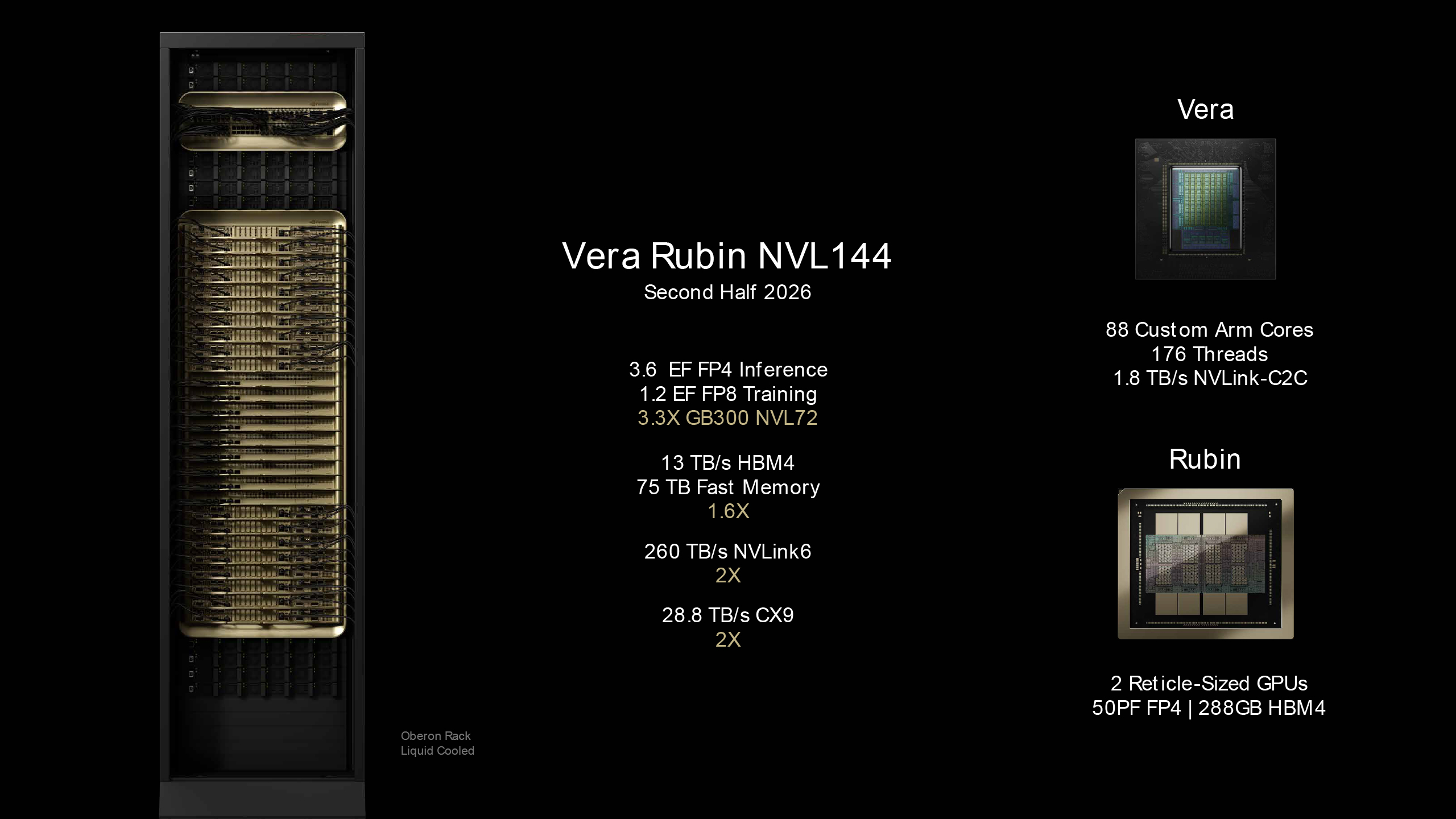
Starting from the second half of 2026, Nvidia plans to roll out its Vera Rubin NVL144 systems, featuring 144 VR200 GPUs, and will largely retain the Oberon architecture. The rationale behind Nvidia's naming scheme will also change for NVL144, as the company will begin counting the number of GPU chiplets as 'GPUs,' instead of the number of GPU packages.
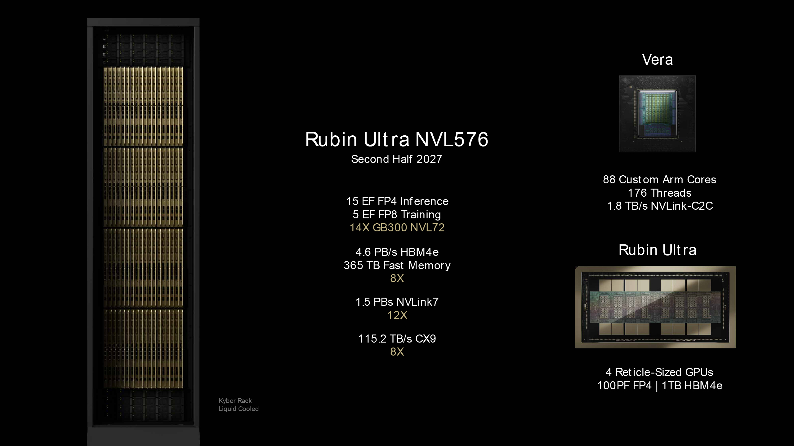
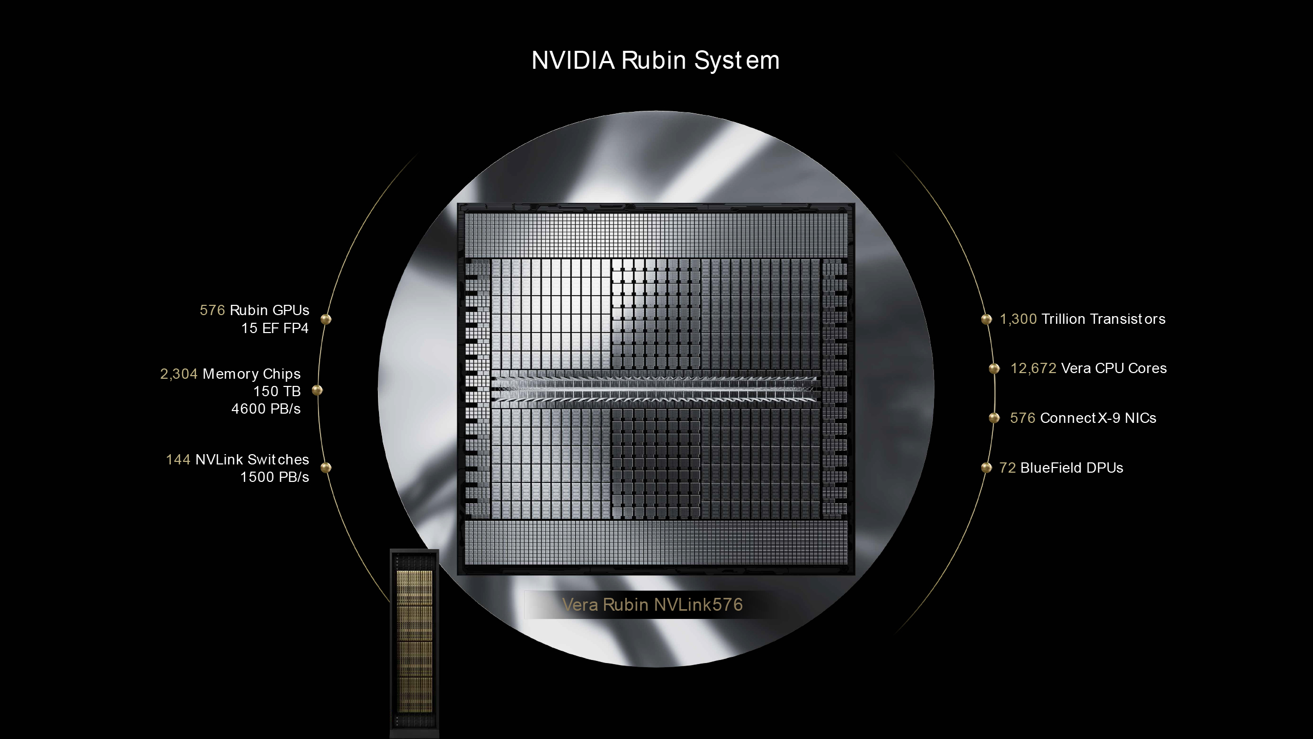
Nvidia is planning to radically improve its system offerings in the second half of 2027. This will be done thanks to its Rubin Ultra NVL576 machine, sporting the 'Kyber' rack, which will pack as many as 144 quad-chiplet Rubin Ultra GPUs, or 576 compute GPU chiplets, as the name suggests.
As the number of GPUs increases, so will their NVLink and networking bandwidth. Nvidia expects its NVL576 machines to provide 14 times the performance of GB300 NVL72 machines for inference and training workloads. The Kyber architecture will be significantly different from existing offerings, but will retain a direct liquid cooling solution, despite much higher power consumption.
Outlook
Thanks to Nvidia's announcements at GTC 2025, we have a good idea of what the company's current enterprise system roadmap looks like. Their ambitious plans span across GPUs, CPUs, interconnects, networking, and systems, signaling a major performance uplift aimed at AI and HPC workloads.
Nvidia's 2025 – 2027 roadmap marks a major leap in AI infrastructure, with GPU performance scaling from the Blackwell B200's 10 FP4 PFLOPS and 192 GB of HBM3 memory to the Rubin Ultra's 100 FP4 PFLOPS and 1 TB of HBM4E memory, as well as skyrocketing power consumption of 3600W per GPU package.
These upcoming GPUs will be paired with 88-core Vera CPUs and next-gen NVLink 7.0 interconnects, delivering 14,400 GB/s per switch, in addition to silicon photonics-based Spectrum-X and Quantum-X networking for ultimate scalability.
By late 2027, Nvidia will also introduce its codenamed 'Kyber' NVL576 systems, which will integrate 576 GPU chiplets per rack, delivering up to 14 times the performance of current NVL72 platforms and redefining compute density for AI.
We will be sure to update our roadmap as we gather and collate new information.

Anton Shilov is a contributing writer at Tom’s Hardware. Over the past couple of decades, he has covered everything from CPUs and GPUs to supercomputers and from modern process technologies and latest fab tools to high-tech industry trends.
