Desktop GPU roadmap: Nvidia Rubin, AMD UDNA & Intel Xe3 Celestial
Where is the desktop GPU market headed? We investigate.
Get Tom's Hardware's best news and in-depth reviews, straight to your inbox.
You are now subscribed
Your newsletter sign-up was successful
The GPU landscape has been buzzing with fresh offerings from all three major desktop GPU brands: Nvidia, AMD, and Intel. All three major manufacturers have completed their current family of GPUs, so we can expect more variants or refreshes in the future.
With the mid-range offerings from both Nvidia and AMD recently hitting the market in the form of the RTX 5050 and RX 9060, both Team Green and Red now have their eyes set on future architectures and technologies.
With so much excitement around new chips and architectures, what’s next for all three companies? We break down everything you need to know about their upcoming plans. We will keep this page consistently updated with the latest information to hand, with accurate sourcing and no rumors.
Article continues belowNvidia
Architecture | Expected Launch | Node | Power |
|---|---|---|---|
Rubin | Q4 2026/Q1 2027 | TSMC N3P | TBC |
Rubin Ultra | H2 2027 | TSMC N3P/3N+ | TBC |
Feynman | TBC | TSMC N2/Intel | TBC |
Currently, the Nvidia RTX 50 series represents the consumer manifestation of the Blackwell architecture, which introduced significant architectural enhancements focused on neural rendering, AI acceleration, and ray tracing performance. Built on TSMC's 4NP process node, the Blackwell consumer GPUs highlighted an uplift in AI-accelerated workloads across desktop and laptop platforms. But it wasn't a huge leap in performance across the board.
Nvidia RTX 50 series GPUs utilize TSMC's custom 4NP process technology, an enhanced variant of the foundry's N4P production node specifically tailored for Nvidia's requirements. This is a continuation of TSMC's 5nm-class manufacturing family, prioritizing mature process reliability over bleeding-edge node adoption, which allows for some degree of cost control.
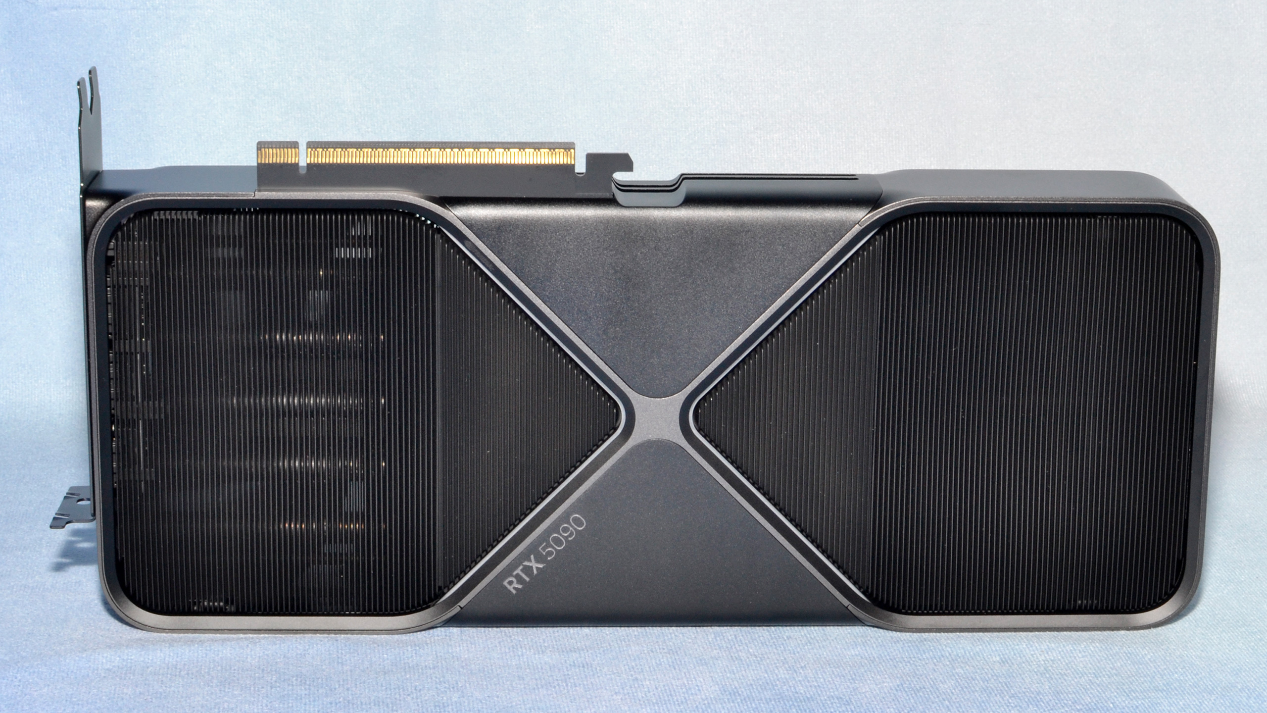
The Blackwell consumer architecture incorporates fundamental architectural improvements over Ada Lovelace, including doubled integer math throughput per clock cycle through fully unified FP32 and INT32 cores. The streaming multiprocessor (SM) design has been completely reengineered, with each SM containing 128 CUDA cores, four fifth-generation Tensor cores, one fourth-generation RT core, and four texture units alongside 256KB register files and configurable 128KB L1/shared memory.
The post-Blackwell era of Nvidia consumer graphics signals a strong shift toward neural rendering-first design philosophy, with three major architectural generations positioned to push the envelope on desktop and laptop GPU capabilities through 2029.
The Rubin, Rubin Ultra, and Feynman architectures plan to incorporate advanced manufacturing processes, next-generation memory technologies, and AI acceleration, which are likely to land in future desktop GPUs.
Nvidia's Rubin architecture detailed
Nvidia's Rubin architecture is expected to be the first consumer GPU generation manufactured on TSMC's 3nm-class process technology. Projected to debut in late 2026 with the RTX 60 series, Rubin will likely transition from TSMC's 4NP node utilized by Blackwell to the more advanced N3P process, delivering significant improvements in transistor density and power efficiency.
As anticipated, the Rubin consumer GPU, powered by TSMC's 3nm node, might provide approximately 15% increased transistor density compared to the 4nm process used for RTX 50 series GPUs. This transition enables TSMC to deliver a claimed 10-15% performance improvement at equivalent power consumption, or offer a 20-30% power reduction at equivalent performance levels. However, whether or not that will hold will have to be confirmed by Nvidia itself.
Rubin GPUs are expected to debut multiple dies: a flagship (e.g., RB102) for top-end cards (RTX 6090), and cut-down dies (RB103/RB104, etc.) for RTX 6080/6070/6060 series. Consumer variants will likely follow the pattern seen in Blackwell and Ada Lovelace.
Expect the largest die for halo product, and cut-down dies for enthusiast/mainstream cards. Laptop variants will use further cut-down dies or lower TDP (Max-Q) implementations. Since Nvidia is continually shifting die cut-downs between generations, it's difficult to pinpoint exactly which might end up turning into a specific GPU class.
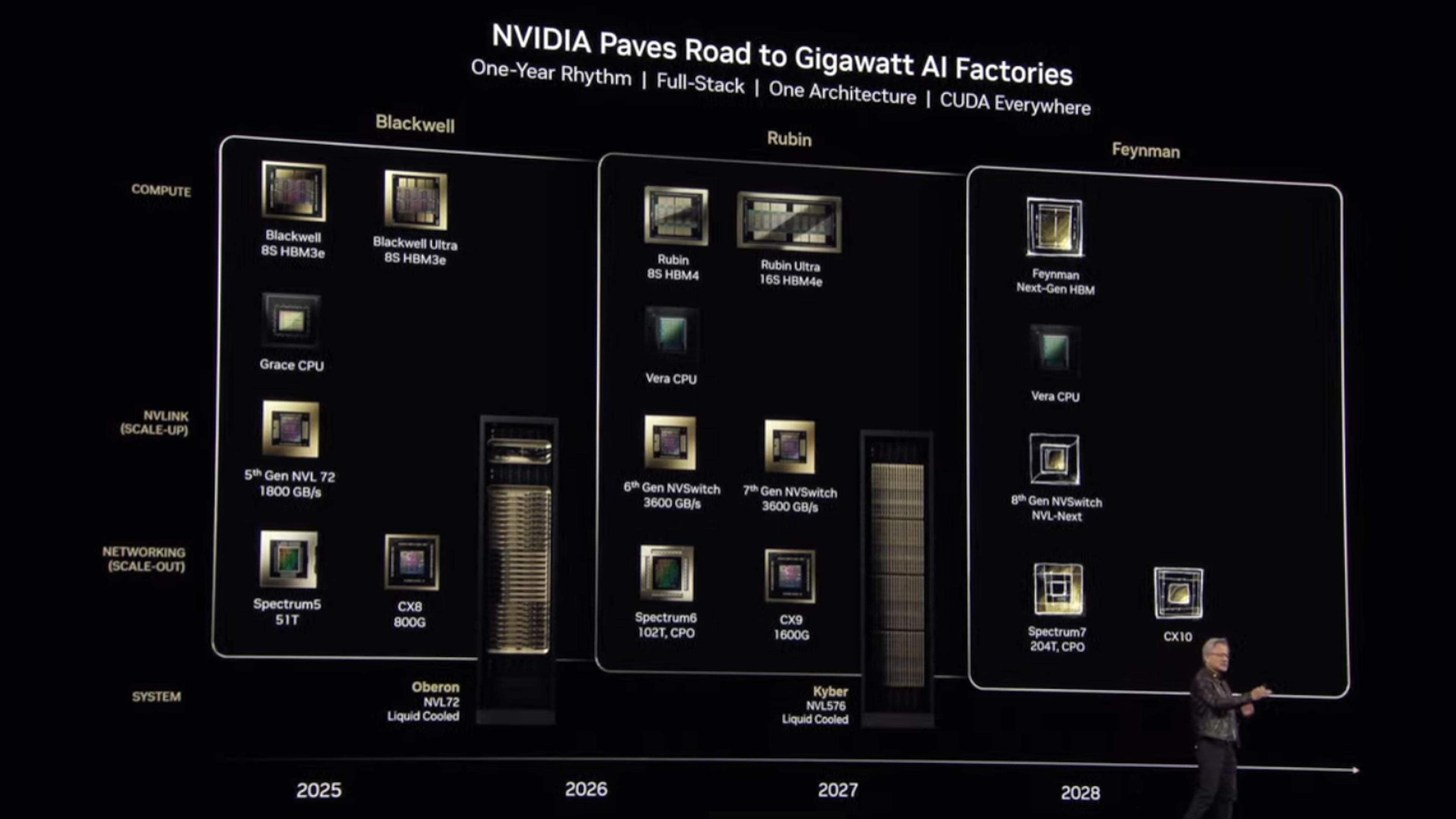
Data center Rubin dies are targeting up to 1,800W per AI chip at the highest configuration. However, consumer desktop models will likely be dramatically lower.
To make an educated guess, the projected desktop power demand puts the flagship RTX 6090 likely in the 450–600W range, scaling down to 200W or less for mainstream models. This is an extrapolation from Blackwell and Ada Lovelace scaling, with increased efficiency due to being powered by a 3nm node.
Nvidia has confirmed that Rubin will use HBM4 in the data center. However, memory configurations for consumer Rubin GPUs are expected to utilize faster GDDR7 variants or potentially introduce GDDR7X memory technology, offering substantial bandwidth improvements over current GDDR7 implementations.
Nvidia's Rubin architecture for desktops is anticipated to be available for the consumer GeForce lineup (RTX 60 series). There is no official indication that Rubin is data center-only; Nvidia’s executive statements and annual release cadence strongly point toward the lineup's release.
Rubin production is on track for H2 2026, per official Nvidia statements and refuted delay rumors. Consumer cards are expected to be available in late 2026 or early 2027, as of the time of writing.
Rubin Ultra (2027) and Feynman (2028)
Following Rubin, there is no official confirmation about the consumer implementation of future architectures announced at GTC 2025, as Nvidia is traditionally an enterprise-first company. However, the architectures (Rubin Ultra and Feynman) may be used in consumer GPUs.
Feynman, like Volta (2017), may remain data center-only, but all current Nvidia statements suggest consumer implementations are planned.
Rubin Ultra, scheduled for the second half of 2027, is slated to be the successor of Rubin. At the data center level, this architecture implements quad-die GPU configurations within single packages, dramatically increasing computational density.
Rubin Ultra's quad-die implementation requires advanced packaging technologies. Whether or not this layout trickles down to consumer GPUs remains to be seen. Consumer implementations will likely utilize cost-optimized packaging approaches while maintaining the performance advantages of multi-die, or chiplet architectures.
The gate-all-around field-effect transistor (GAAFET) technology implementation in TSMC's 2nm variant, expected for Rubin Ultra and possibly Feynman, represents a significant departure from FinFET designs, offering enhanced optimization flexibility for either performance or efficiency targets.
Data center implementations of Rubin Ultra are currently planned to have HBM4/HBM4e memory, but it is unlikely that HBM will end up being the VRAM type used in consumer GPUs based on the Rubin Ultra and Feynman architectures.
Feynman is the company's most advanced GPU generation currently planned. Limited official information exists regarding Feynman's consumer specifications, though data center roadmaps provide architectural insights that may apply to consumer implementations.
Feynman will likely utilize either TSMC's 2nm node (N2) or potentially Intel's advanced foundry processes, including 18A or 14A nodes. The architecture will likely incorporate seventh-generation Tensor cores and sixth-generation RT cores. Details on Feynman are still light, with Nvidia expected to reveal further details at future events.
Regarding an anticipated launch timeline, Rubin Ultra may launch in the second half of 2027, while Feynman GPUs are still very far off, so don't expect anything sporting the architecture until H2 2028 / H1 2029, at the very earliest. Be sure to take these dates with a dose of salt, as nothing is confirmed until Nvidia itself says so.
AMD
Architecture | Expected Launch | Process Technology | Memory Type | Power |
|---|---|---|---|---|
UDNA/RDNA 5 | Late 2026 - Early 2027 | TSMC 3nm / N3E | GDDR7 (up to 32 Gbps) | TBC |
UDNA 2 / RDNA 6 | 2028+ | TBC | GDDR7X or next-gen VRAM | TBC |
AMD unveiled its RDNA 4 architecture in January 2025, followed by the RX 9000 series of cards in early March. AMD’s primary goal this generation was to target the mainstream with GPUs, in quantity, that were both affordable and performed well.
Departing from its iconic ‘XX00’ naming style in favor of the ‘X0X0’ convention for the mainstream, aligned AMD's branding style with Nvidia. AMD also elected not to introduce any enthusiast-class GPUs with RDNA 4. As such, the RX 9070 XT, which likely utilizes the fully-enabled Navi 48 chip (referred to internally as Navi 48 XTX), represents the most powerful GPU we’ll get with RDNA 4.
AMD has confirmed ongoing R&D for post-RDNA 4 architectures in several presentations, emphasizing continuous improvements in compute density and AI acceleration. Codenames are not yet public, but technical documentation references “Next-Gen RDNA” under the “Growth Driver” umbrella.
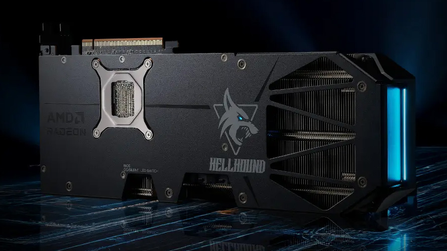
AMD's discrete GPU strategy beyond the current RDNA 4 (RX 9000 series) generation centers on a significant architectural transition, moving from the established Radeon DNA (RDNA) lineage towards a potentially unified architecture, internally designated GFX13. Crucially, AMD has publicly confirmed the development of an architecture following RDNA 4 during its Financial Analyst Day 2022 and subsequent roadmap updates, though specific branding (RDNA 5 vs. UDNA) remains officially unclarified.
UDNA / RDNA 5: AMD's next-generation GPU architecture
While AMD roadmaps historically labeled this successor "RDNA 5," current industry reports suggest a potential rebranding to "UDNA" (Unified DNA). This signifies a strategic shift towards a single architecture foundation targeting both consumer gaming (replacing RDNA) and compute/data center workloads (replacing CDNA).
AMD publicly emphasizes the challenge and resource drain of maintaining two distinct architectures (RDNA for gaming, CDNA for compute). A unified UDNA architecture aims to simplify the software stack (particularly ROCm), improve memory optimization consistency, and enhance forward/backward compatibility across the products, from laptops to servers.
AMD aims to streamline development, hardware design, and software optimization by adopting a consistent core Arithmetic Logic Unit (ALU) design reminiscent of the pre-RDNA Graphics Core Next (GCN) lineage, enabling compatibility across consumer gaming, AI workloads, and professional compute workloads alike.

Crucially, UDNA is expected to be fabricated on TSMC’s 3nm-class manufacturing node (N3 or N3E). This will represent a substantial leap in transistor density and power efficiency over RDNA 4’s 5nm process node.
AMD has publicly stated that improving ray tracing performance is a core focus for future generations. RDNA 5/UDNA is projected to feature significantly redesigned Ray Accelerators, potentially moving more fixed-function hardware into the pipeline to alleviate shader engine burden and dramatically increase ray intersection throughput compared to RDNA 4.
The UDNA architecture may also see AMD shift back from monolithic to a chiplet-based design, optimizing manufacturing yields and enabling finer die cutdowns. AMD already employs a technique allowing it to produce more SKUs from a single silicon design through a technique named asymmetric harvesting. Potentially using this, can expect a range from 96 CUs all the way down to 32 CUs for UDNA, with GDDR7 memory being the VRAM technology of choice.
We expect UDNA to debut in late 2026. Broader availability across desktop segments and mobile variants (RX 10000M series) might arrive in Q1-Q2 2027. However, this remains unconfirmed. We expect to hear official details on UDNA at AMD's 2025 Financial Analyst Day in November 2025.
Intel
Architecture | Expected Launch | Process Node | Compute Units (Max) | Memory Type | Power |
|---|---|---|---|---|---|
Xe3 Celestial | 2026 - Early 2027 | Intel 18A | TBC | TBC | TBC |
Xe4 Druid | Late 2027 - 2028 | TBC | TBC | TBC | TBC |
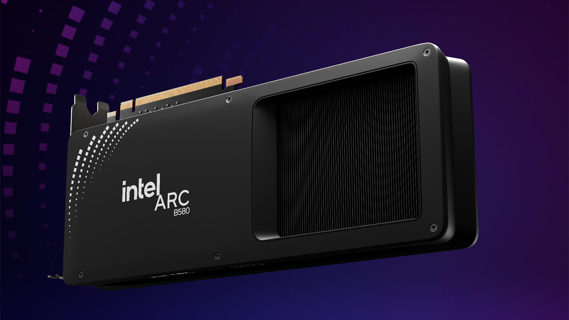
Intel officially launched its second-generation discrete GPU family, namely Battlemage (Xe2), with the Arc B580 and Arc B570 in December 2024 and January 2025, respectively. Despite some teething issues, these GPUs were surprisingly capable, affordable, and generously equipped with 12GB/10GB of VRAM, capacities that are unheard of in the $250 market.
Intel has officially established its commitment to discrete graphics beyond the current Battlemage generation, with Co-CEO Michelle Johnston Holthaus confirming at CES 2025 that Intel remains "very committed to the discrete graphics market" and will "continue to make strategic investments".
With the Battlemage (Xe2 architecture) now deployed, Intel's roadmap extends through the Xe3 "Celestial" and Xe4 "Druid" architectures, representing significant steps in Intel’s GPU design and manufacturing strategy.
Xe3 Celestial and Xe4 Druid
Intel Fellow Tom Petersen confirmed in December 2024 that the Xe3 Celestial architecture has been finalized, with hardware design locked and the development team transitioning to Xe4 development. Intel has not disclosed full architectural details, but Xe3 builds on Xe2's vector engines with projected refinements in compute throughput and cache hierarchies.
Celestial has progressed to pre-silicon validation as of May 2025, with Intel's OEM partners conducting virtual GPU testing for firmware development. Based on Intel's validation timeline, Celestial is expected to enter volume production by late 2025 or early 2026.
Celestial will initially debut as integrated graphics within Intel's Panther Lake mobile processors, likely utilizing Intel's 18A process node. While Intel has not officially disclosed the target process node, its alignment with the Panther Lake CPU platform (built on Intel 18A) suggests a high probability that the initial Celestial variants will utilize the same node.
Intel's focus on AI acceleration suggests higher memory capacities will be prioritized to support emerging AI inference workloads alongside traditional gaming applications.
Discrete Celestial GPUs are not expected until after the architecture debuts in integrated form within Panther Lake mobile CPUs. Based on typical development cycles, volume production of discrete Celestial GPUs might not begin until late 2026, with availability beginning in early 2027. However, this remains unconfirmed until Intel itself offers up more information.

For Xe4 Druid, Intel has confirmed hardware work is underway, as Petersen noted, "The hardware teams are off on to the next thing (Xe4)". This architecture is projected as a modular redesign, potentially incorporating hybrid tiles for graphics and media, as hinted in Intel's June 2025 leaks on Nova Lake iGPUs using Xe3/Xe4 combinations, though discrete details are absent.
Petersen also noted that Intel's development lifecycles can exceed one year, meaning that it's likely that we won't see this particular architecture materialize for desktop system use for quite some time, so don't hold your breath for Druid until 2026, or beyond.
We will continue to keep this page updated as soon as we hear any official details.

Hassam Nasir is a die-hard hardware enthusiast with years of experience as a tech editor and writer, focusing on detailed CPU comparisons and general hardware news. When he’s not working, you’ll find him bending tubes for his ever-evolving custom water-loop gaming rig or benchmarking the latest CPUs and GPUs just for fun.
