Kioxia's next-gen 3D NAND production gets expedited to 2026, report claims — high-capacity 332-layer BiCS10 devices to sate growing demand from AI data centers
Mass production of 332-layer BiCS10 accelerated from 2027 to 2026.

Get Tom's Hardware's best news and in-depth reviews, straight to your inbox.
You are now subscribed
Your newsletter sign-up was successful
Kioxia will produce its next-generation BICS9 and BICS10 3D NAND memory next year, but will use different fab sites for different types of flash, according to Nikkei. BiCS10 transitions to an all-new 332-layer 3D NAND array to address high-capacity solutions for AI and hyperscalers.
Perhaps the biggest surprise about 332-layer BiCS10 is that Kioxia (and Sandisk) is pulling in production of this type of memory to 2026, if the Nikkei report is correct. The publication states that both companies initially planned to produce BiCS10 memory in the second half of 2027. However, demand from the AI, cloud, and enterprise sectors likely prompted Kioxia to begin production ahead of schedule for its most advanced memory announced to date.
While both BICS9 and BICS10 use the CBA (CMOS directly Bonded to Array) architecture and boast a 4.8 GT/s Toggle DDR 6.0 interface, BICS9 uses a smaller 218-layer 3D NAND array to target performance-hungry low-power applications.
Different fabs for different memory
As noted above, Kioxia (and therefore Sandisk) will use different fab sites to make BiCS9 and BiCS10 3D NAND. Specifically, the newest Fab 2 near Kitakami, Iwate prefecture, will become the base for making high-capacity 332-layer BiCS10 NAND, whereas the established complex near Yokkaichi in Japan's Mie prefecture will remain the center for 218-layer BiCS9 3D NAND.
The decision to produce flagship BiCS10 devices at Fab 2 in Iwate Prefecture makes a lot of sense, as the site has the latest equipment, even though Kioxia's R&D center is in Yokkaichi. However, the fabs in Yokkaichi are still good enough (and largely depreciated) for BiCS9, will address mainstream devices, and must be cost-effective to manufacture.
Keep in mind that the information is largely unofficial and unconfirmed by Kioxia and Sandisk; many details are subject to change ahead of an official announcement.
CBA: The key to next-generation 3D NAND
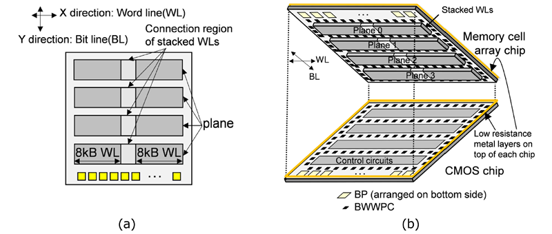
Developing high-speed memory interfaces for 3D NAND is challenging, so leading flash memory suppliers have taken a page from Yangtze Memory's playbook. Companies have begun producing memory arrays and peripheral CMOS logic responsible for memory operations on separate layers. These are then attached together using hybrid-bonding techniques. Kioxia and Samsung call their architecture CMOS Directly Bonded to Array (CBA) and have been deploying the technique since BiCS8 3D NAND, which started production in the second half of 2024.

The companies plan to continue using CBA with BiCS9 and BiCS10, but this time around, adopting an 8-bit Toggle DDR 6.0 interface with a 4.8 GT/s data transfer rate (600 MB/s). This is done to increase performance to unprecedented levels for both generations of 3D NAND, which are set to coexist in the market, targeting different applications.

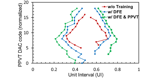
Kioxia’s Toggle DDR 6.0 interface combines three elements: an unmatched DQS timing scheme, per-pin VREF training (PPVT), and a compact 2-way decision-feedback equalizer (2TI-DFE). Each data pin (DQ [7:0]) has its own calibrated reference voltage, enabling the receiver to detect bits at 4.8 Gbps correctly.
Instead of using the heavier 4-way interleaved DFE used in DRAM interfaces, Kioxia implemented a 2-way version with a Data-Driven Self-Reset (DDSR) circuit. This holds the previous decision values (OP and OM) until it detects a polarity change via a small 3-input NAND gate, preventing incorrect feedback and reducing both area and power.

On the timing side, the Toggle DDR 6.0 interface uses an unmatched DQS structure with PPVT and a simplified 2TI-DFE to simplify timing alignment while still enabling deterministic data read windowing. This cooperation extends the safe sampling window for incoming data without requiring additional analog hardware, which is costly in terms of power and transistor budget. Shmoo plots for all eight data lines confirm that the interface should stay reliable at 4.8 GT/s with this design.
BiCS9: 218L 3D NAND meets Toggle DDR 6.0 at 4.8 GT/s
Implementing both a very high-speed interface and an all-new 3D NAND array with 332 active layers is a costly project that yields high-performance, high-capacity 3D NAND that not all applications actually require. To that end, BiCS9 combines the proven 218-layer 3D NAND array with the NAND interface at 4.8 GT/s.
As Sandisk calls it, BiCS9 will power 'capital-efficient, high-performance, low-power products,' which primarily includes cost-sensitive client storage solutions such as those used in PCs and smartphones, as well as products that require pure performance, and do not need the highest capacity or storage density available.
Perhaps, once yields of 332-layer 3D NAND match those of 218-layer 3D NAND, Kioxia and Sandisk will transition to the new process technology and lower their costs. For now, it makes more sense for both companies to reserve the 332-layer 3D NAND array for applications requiring maximum storage density and capacity.
BiCS10: 332L 3D NAND with lower latency and lower power meets Toggle DDR 6.0 at 4.8 GT/s
While 332-layer BiCS10 3D NAND increases bit density by a whopping 59% to 29 Gb/mm^2, this isn't the only improvement the new type of memory offers, as it also shrinks read latency by around 4 microseconds, and reduces read power consumption by 29%, from around 100 mj per GB to near 75 mj per GB.

Based on Kioxia's description, the company has boosted read performance in BiCS10 3D NAND by changing how the unselected word lines (WLs) behave during continuous reads. In a very tall 332-layer stack, most of the delay and energy cost comes from repeatedly charging long WL strings from VSS up to VREAD.

Normally, after each read, the internal read voltage fully drops to ground and then climbs back to VREAD for the next cycle, which takes time and draws significant current. Kioxia's new method avoids that full swing: after the first read, the circuit lowers VREAD only to an intermediate level (still above VSS), and then, before the next read, raises it back to the full read voltage. Because the WLs move over a smaller voltage range, the array charges faster and consumes less current. Such an architecture makes the read path more efficient and better suited for continuous-access workloads, which is crucial for high-layer NAND dies.

Anton Shilov is a contributing writer at Tom’s Hardware. Over the past couple of decades, he has covered everything from CPUs and GPUs to supercomputers and from modern process technologies and latest fab tools to high-tech industry trends.
