
Avid readers of Tom’s Hardware have read a lot about the upcoming HBM4 and GDDR6 memory technologies, but as neither is used on mass production devices, few of us get to see actual HBM4 and GDDR6 memory packages. Good news, SK Hynix demonstrated them at CES, and our own Matt Safford has managed to grab some pictures.
SK Hynix demonstrated the industry’s first 16-Hi HBM4 memory package at the trade show, highlighting both the density that could not be achieved without its MR-MUF molding technology as well as HBM4’s 2,048-bit interface. SK hynix's HBM4 memory stacks are said to operate at 10 GT/s, which is 25% faster than the official JEDEC specification. Meanwhile, adopters like Nvidia want to have headroom for both extra performance in scale-up deployments (if customers are willing to) and for performance efficiency in hyperscaler applications.
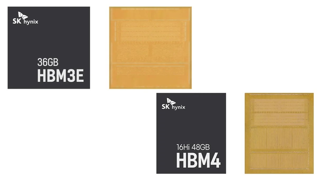
HBM3/HBM3E and HBM4 share the same ~10.5 × 12.0 mm footprint, but HBM4 allows taller stacks — up to ~950 µm for 16-Hi versus ~750 µm for 12-Hi HBM3 — while packing far denser I/O and power bumps. When it comes to packaging, the company continues with its advanced mass Reflow molded underfill (MR-MUF) approach: multiple memory dies are mounted on a base substrate and bonded in a single reflow step, then encapsulated with mold material between DRAM layers, the base die, and the substrate.
Looking at the backsides of HBM4 and HBM3E, the difference between them becomes obvious, even taking the general pin count aside. HBM3E and HBM4 feature the same dimensions/footprint, so the backside indeed shows a much denser and more uniformly packed BGA pin field with noticeably higher bump density across the entire footprint. This is not particularly surprising as the jump from a 1,024 to a 2,048-bit I/O takes its obvious toll and requires substantially more signal bumps as well as additional power and ground pins to support higher bandwidth and tighter signal integrity margins. By contrast, HBM3E's backside has a sparser bump layout with more visible separation between regions, which is consistent with its 1,024-bit interface and lower aggregate I/O demand.
Meanwhile, HBM4's power delivery and ground contacts are also visibly different compared to the less advanced type of memory. Perhaps HBM4 allocates a larger fraction of its backside area to power and ground bumps; they are arranged more evenly across the package, something that could reduce noise and IR drop at data rates that are as high as 8 GT/s per standard or 10 GTs, given the listed capability.
Yet, we may be speculating here purely based on the fact that HBM3E features fewer power pins and shows clearer zoning between I/O and power regions. In fact, even without precise specs, the backside alone shows that HBM4 is designed for much higher I/O bandwidth and power delivery requirements.
In any case, these HBM4 modules use custom DRAM dies manufactured on the proven 1b-nm (5th-generation 10-nm-class) process to wed a large DRAM die with low defect density, reduced variability, and eventually high yield, something that makes them cheaper, yet it is hard to estimate how that lower cost could translate to the end user.

Follow Tom's Hardware on Google News, or add us as a preferred source, to get our latest news, analysis, & reviews in your feeds.
