SK hynix completes development of next-gen HBM4 — 2,048-bit interface and 10 GT/s speeds promised for next-gen AI accelerators
Above and beyond JEDEC specifications.


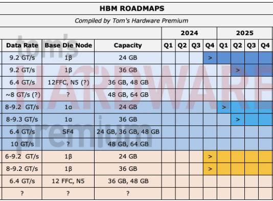
Want more? We've got an exclusive roadmap to the future of high-bandwidth memory — only for subscribers of Tom's Hardware Premium.
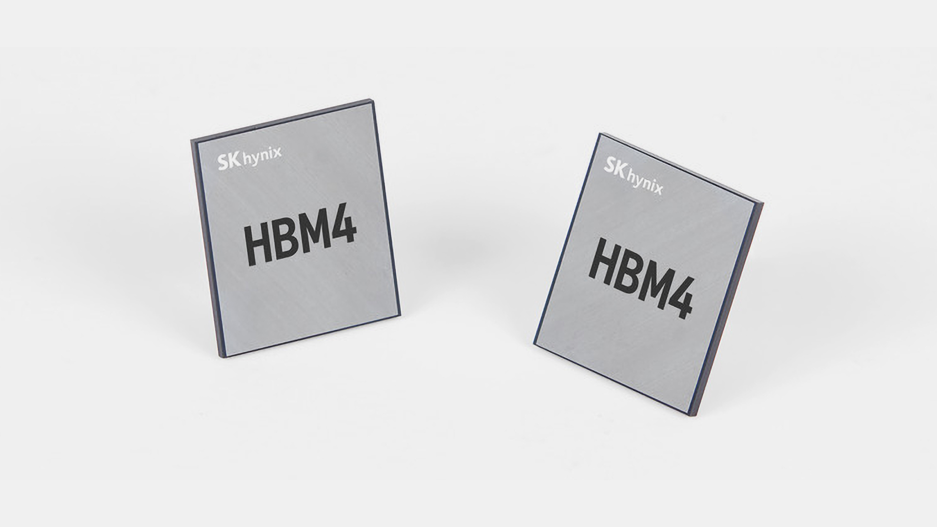
SK hynix has completed development of its HBM4 memory and prepared it for high-volume manufacturing of memory stacks, the company said on Friday. HBM4 stacks from SK hynix go beyond specifications set by JEDEC by 25% in terms of performance, though it remains to be seen whether producers of next-generation AI accelerators — such as AMD, Broadcom, or Nvidia — will use that potential on their 2026 products.
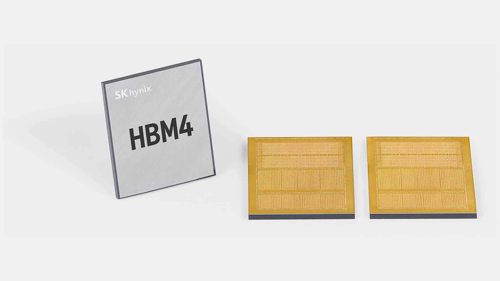
SK hynix’s HBM4 memory stacks feature a 2,048-bit I/O, doubling the width of the HBM interface for the first time since 2015, and a 10 GT/s data transfer rate, which is 25% higher compared to the official JEDEC standard (more on this later). The company's HBM4 memory stacks use specially designed DRAM dies built using proven 1b-nm (5th Generation 10nm-class) process technology that combines decent performance efficiency with node maturity (i.e., low defect density and variability).
For its HBM4 modules, SK hynix continues to use its proven Advanced Mass Reflow Molded Underfill (MR-MUF) method. In this process, multiple memory chips are placed on a base substrate and bonded together in a single reflow step. Right after that, spaces between the stacked DRAM layers, base die, and substrate are filled with a mold material to secure and protect the structure. Advanced MR-MUF enables the company to keep the height of its 12-Hi HBM stacks within specification and improve heat dissipation of power-hungry memory modules.
"Completion of HBM4 development will be a new milestone for the industry," Joohwan Cho, Head of HBM Development at SK hynix, who has led the development, said. "By supplying the product that meets customer needs in performance, power efficiency and reliability in timely manner, the company will fulfill time to market and maintain competitive position."
Unfortunately, SK hynix does not disclose either how many DRAM layers its HBM4 devices use, or their capacity, though we are likely talking about 12-Hi 36 GB devices that will be used for Nvidia's Rubin data center GPUs, but we are speculating. The company also does not disclose whether its initial HBM4 stacks use 12FFC+ (12nm-class) or N5 (5nm-class) base logic dies produced by TSMC.
Arguably, the most interesting part of SK hynix's announcement is the fact that it decided to go beyond JEDEC's specification and certify its HBM4 stacks for a 10 GT/s data transfer rate, up from the 8 GT/s set by the standard. The company is not alone in going beyond JEDEC spec with HBM4: Micron is currently sampling HBM4 devices with a 9.2 GT/s data transfer rate, whereas Rambus has an HBM4 memory controller capable of 10 GT/s speed. While extra performance may be used by actual chip developers at some point, most developers apparently want to have some reserve for added piece of mind, according to an insight shared by Rambus a few years ago.
SK hynix says that it is ready to mass produce its HBM4 stacks, though it does not disclose when it plans to kick off volume production of HBM4.
Get Tom's Hardware's best news and in-depth reviews, straight to your inbox.
"We are unveiling the establishment of the world’s first mass production system of HBM4," said Justin Kim, President & Head of AI Infra at SK hynix. "HBM4, a symbolic turning point beyond the AI infrastructure limitations, will be a core product for overcoming technological challenges. We will grow into a full-stack AI memory provider by supplying memory products with the best quality and diverse performance required for the AI era in a timely manner."
Follow Tom's Hardware on Google News, or add us as a preferred source, to get our up-to-date news, analysis, and reviews in your feeds. Make sure to click the Follow button!

Anton Shilov is a contributing writer at Tom’s Hardware. Over the past couple of decades, he has covered everything from CPUs and GPUs to supercomputers and from modern process technologies and latest fab tools to high-tech industry trends.
