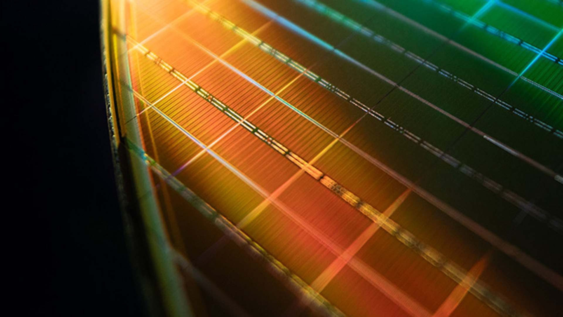
'Beyond EUV' chipmaking tech pushes Soft X-Ray lithography closer to challenging Hyper-NA EUV — 'B-EUV' uses new resist chemistry to make smaller chips
But will it ever materialize?

Get Tom's Hardware's best news and in-depth reviews, straight to your inbox.
You are now subscribed
Your newsletter sign-up was successful
Researchers at Johns Hopkins University have unveiled a new approach to chipmaking that uses lasers with a 6.5nm ~ 6.7nm wavelength — also known as Soft X-rays — that could increase the resolution of lithography tools to 5nm and below, reports Cosmos, citing a paper published in Nature.
The scientists call their method 'beyond-EUV' — suggesting that their technology could replace industry-standard EUV lithography — but the researchers admit they are currently years away from building even an experimental B-EUV tool.
Soft X-Rays can challenge Hyper-NA. On paper
The most advanced chips nowadays are made using EUV lithography, which operates at a wavelength of 13.5 nm and can produce features as small as 13nm (Low-NA EUV of 0.33 numerical aperture), 8nm (High-NA EUV of 0.55 NA), or even 4nm ~ 5nm (Hyper-NA EUV on 0.7 – 0.75 NA) at the cost of extreme complexity of the lithography systems that have very advanced optics that cost hundreds of millions of dollars.
Article continues belowBy using a shorter wavelength, researchers from Johns Hopkins University can get an intrinsic resolution boost even with lenses with moderate NA. However, they face many challenges with B-EUV.
Firstly, B‑EUV light sources are not yet ready. Various researchers have tried multiple methods of generating 6.7 nm wavelength radiation (e.g., gadolinium laser-produced plasma), but there is no industry-standard approach. Secondly, these shorter wavelengths — due to their high photon energy — interact poorly with traditional photoresist materials used in chipmaking. Thirdly, because 6.5nm ~ 6.7nm wavelength light is absorbed rather than reflected by pretty much everything, multilayer-coated mirrors for this type of radiation haven't been produced before.
Lithography Type | Wavelength | Achievable Resolution | Photon Energy | Numerical Aperture (NA) | Notes |
g-line (Pre-DUV) | 436 nm | 500 nm | 2.84 eV | 0.3 | Uses mercury vapor lamps; legacy nodes; low resolution. |
i-line (Pre-DUV) | 365 nm | 350 nm | 3.40 eV | 0.3 | Used for early CMOS. |
KrF DUV | 248 nm | 90 nm | 5.00 eV | 0.7 - 1.0 | Used from ~130 nm to 90 nm; excimer laser source; still used in backend layers. |
ArF DUV | 193 nm | 65 nm (dry) - 45 nm (immersion + multipatterning) | 6.42 eV | Up to 1.35 (immersion) | Most advanced DUV; still essential in multi-patterned 7 nm–5 nm nodes; used for many layers in 2nm nodes. |
EUV | 13.5 nm | 13 nm (native), 8 nm (multi-patterning) | 92 eV | 0.33 | In volume production for 5nm - 2nm nodes. Will be used for years to come. |
High-NA EUV | 13.5 nm | 8 nm (native), 5 nm (extended) | 92 eV | 0.55 | First tools: ASML EXE:5200B; targets beyond 2 nm-class nodes; reduced field size, higher cost. |
Hyper-NA EUV (future) | 13.5 nm | 4 nm or better (theoretical) | 92 eV | 0.75 or more | Future tech; requires exotic mirrors and ultra-high precision engineering. |
Soft X-ray / B-EUV | 6.5 nm - 6.7 nm | less than 5 nm (theoretical) | 185-190 eV | 0.3 - 0.5 (expected) | Experimental; high-energy photons; new metal-organic resist chemistries under test. |
Finally, these lithography tools must be designed from scratch, and currently, there is no ecosystem to support the designs with components and consumables. To sum up, building a B-EUV machine (or Soft X-ray machine?) requires breakthroughs in light sources, projection mirrors, resists, and even consumables like pellicles or photomasks.
Solving challenges one at a time
Researchers at Johns Hopkins University, led by Professor Michael Tsapatsis, explored how certain metals can improve the interaction between B-EUV (around 6 nm wavelength) light and resist materials used in chipmaking (i.e., they did not work on other challenges associated with Soft X-rays).
Get Tom's Hardware's best news and in-depth reviews, straight to your inbox.
The team discovered that metals like zinc are able to absorb B-EUV light and emit electrons, which then trigger chemical reactions in organic compounds called imidazoles. These reactions make it possible to etch very fine patterns onto semiconductor wafers.
Interestingly, while zinc performs poorly with traditional 13.5nm EUV light, it becomes highly effective at shorter wavelengths, highlighting how important it is to match the material with the right wavelength.
To apply these metal–organic compounds to silicon wafers, the researchers developed a technique called chemical liquid deposition (CLD). This method creates thin, mirror-like layers of a material called aZIF (amorphous zeolitic imidazolate frameworks), growing at a rate of 1nm per second. CLD also allows for fast testing of different metal–imidazole combinations, making it easier to discover the best pairings for different lithography wavelengths. While zinc is well suited for B-EUV, the team noted that other metals might perform better at different wavelengths, offering flexibility for future chipmaking technologies.
This approach gives manufacturers a toolbox of at least 10 metal elements and hundreds of organic ligands to create custom resists tailored to specific lithography platforms, the researchers disclosed.
Summary
Although the researchers did not solve the full stack of B-EUV challenges (e.g., source power, masks), they advanced one of the most critical bottlenecks: finding resist materials that can work with 6nm wavelength light. They created the CLD process to apply thin, uniform films of amorphous zeolitic imidazolate frameworks (aZIFs) onto silicon wafers. They experimentally showed that certain metals (like zinc) can absorb Soft X-ray light and emit electrons that trigger chemical reactions in imidazole-based resists.
There are plenty of challenges to be solved with B-EUV, and the technology doesn't have a clear path to the mass market. However, the CLD process can be used pretty widely, both in semiconductor and non-semiconductor applications.
Follow Tom's Hardware on Google News, or add us as a preferred source, to get our up-to-date news, analysis, and reviews in your feeds. Make sure to click the Follow button!

Anton Shilov is a contributing writer at Tom’s Hardware. Over the past couple of decades, he has covered everything from CPUs and GPUs to supercomputers and from modern process technologies and latest fab tools to high-tech industry trends.