ASML has now fired back at criticism from analysts at SemiAnalysis who believe that, for at least some chipmakers, using the company's next-gen High-NA chipmaking tools makes little financial sense. However, in a recent interview with Bits and Chips, the company's CFO said that High-NA is on track and healthy and that the analyst firm has underestimated its benefits. During the company's recent earnings call, ASML's CEO also responded to questions about the report, saying the new tech is "very clearly the most cost-effective solution both in logic and memory.”
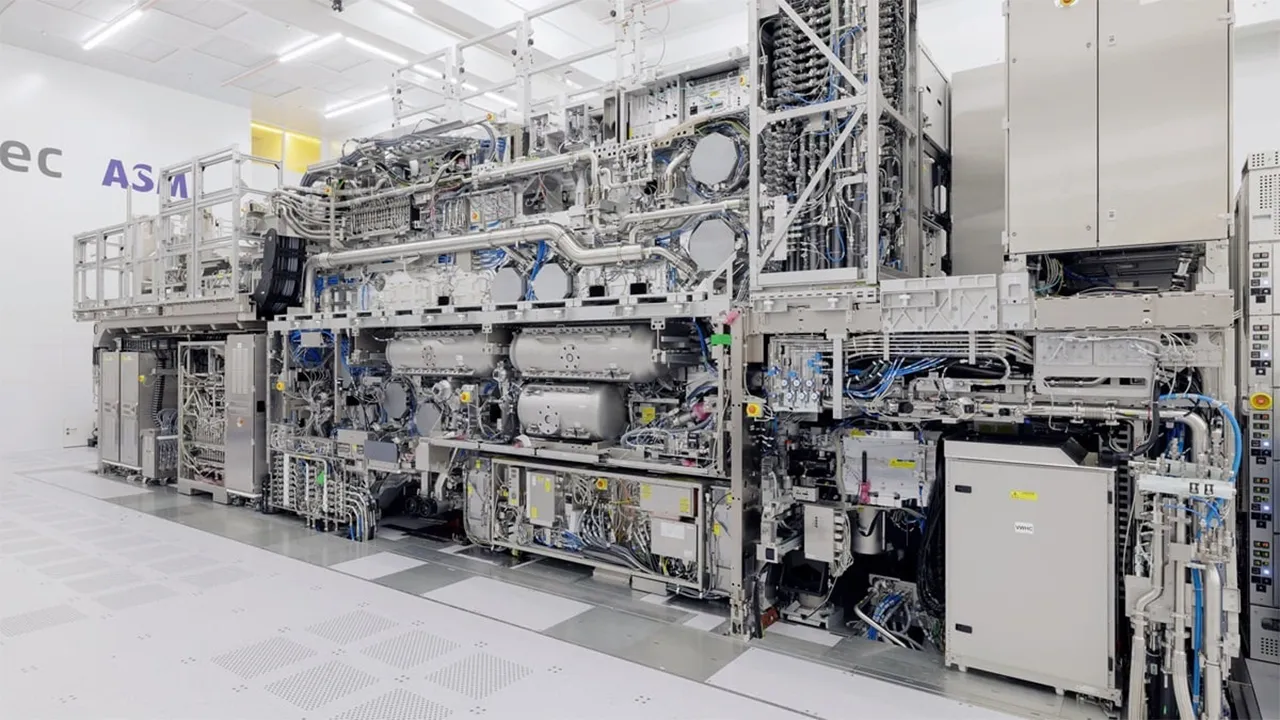
ASML's Twinscan EXE High-NA EUV lithography tools are vital for producing next-generation process technologies smaller than 2nm. But they are also significantly more expensive than existing Twinscan NXE Low-NA extreme ultraviolet (EUV) lithography tools — some say they cost between $300 million and $400 million. They also have other peculiarities, such as halved reticle size and large dimensions, which is part of the reason some analysts contend the tools aren't economically viable for all production lines.
As one would expect, ASML disagrees with that assessment, with the company's CFO telling Bits and Chips that orders are matching the company's expectations and that SemiAnalysis has underestimated the value of reducing process complexity by avoiding costly double- and quadruple-patterning. He also said that one could simply speak with Intel about the complications imposed by double-patterning, a reference to Intel's failures with 10nm which were at least partially due to a lack of EUV technology, to gain an understanding of the difficulties. In fact, Intel is the lead customer for High-NA today, having recently received the first parts of the first High-NA machine shipped to a customer. Let's take a closer look at the issues.
Simpler Manufacturing
Double- and quadruple-patterning involves repeatedly exposing the same layer of a wafer multiple times to create smaller features than normally possible, but it introduces chances for defects, which impacts yields and is more costly than simply printing the layer with one step.
The overall cost of double- and quadruple-patterning with Low-NA tools, and how that compares to single-patterning with a High-NA tool, appears to be one of the primary points of contention between ASML and the analysts.
By now, an eager reader would have probably asked why all the hassle with High-NA EUV if Low-NA EUV tools can achieve the same critical dimensions as the former by using double patterning and/or pattern shaping tools? Indeed, Intel is inserting Applied Materials's Centura Sculpta pattern shaping tool into its Intel 20A flow to avoid costly EUV double patterning in some cases. Meanwhile, Intel 18A indeed relies on both Centura Sculpta pattern shaping and Twinscan NXE double patterning.
But EUV double patterning may not be that bad. Apple uses TSMC's N3B process technology, which reportedly uses double-patterning, for its mass-market products, which include hundreds of millions of iPhone 15 Pros and M3-based Macs.
ASML believes that implementing double patterning incurs certain drawbacks: EUV double patterning leads to longer production times, creates more chances for defects to occur, and potentially impacts the performance variability of produced chips. However, with the EXE:5000's critical dimension (CD) of 8nm, chipmakers can streamline their manufacturing processes.
Foundries certainly understand both the pros and cons of using High-NA EUV scanners, so they are starting their research and development work already.
"Our customers will start their R&D in 2024–2025 and move into high-volume manufacturing in 2025–2026," a statement by ASML reads.
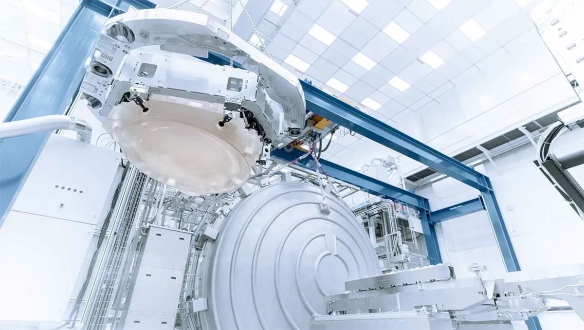
ASML recently shared more details about its new High-NA machines; here's the rundown of how the tools work.
New Tools are Incoming (and Needed)
ASML's next-generation Twinscan EXE has a 0.55 numerical aperture (NA) lens, so it's set to achieve a resolution of 8nm (critical dimension), marking a substantial advancement from the current EUV tools that offer a 13nm resolution. That means it can print transistors 1.7 times smaller – and therefore achieve transistor densities 2.9 times higher – than they can with Low-NA tools with a single exposure.
Low-NA litho systems can achieve a similar resolution, albeit with two exposures, with a costly double-patterning process. Achieving critical dimensions of 8nm is crucial for the production of chips using sub-3nm process technologies, which the industry plans to adopt between 2025 and 2026.
High-NA EUV implementation promises to enable fabs to sidestep the need for EUV double patterning, simplifying the processes, possibly improving yields, and reducing costs. But it brings a lot of challenges, too.
Halved Exposure Field
Meanwhile, ASML's Twinscan EXE lithography tools, equipped with a 0.55 NA lens, completely differ from existing machines. The main and obvious difference is indeed the new and larger lens. But the adaption of a bigger lens requires larger mirrors, which is why Twinscan EXE tools also feature an anamorphic optics design.
This approach addresses the issue of larger mirrors causing light to strike the reticle at a steeper angle, which reduces reflectivity and hinders pattern transfer to the wafer.
Instead of uniformly shrinking the pattern, the anamorphic optics magnify it differently: 4x in one direction and 8x in the other. This reduces the light's angle of incidence on the reticle, solving the reflectivity problem. Additionally, this method allows chipmakers to continue using standard-sized reticles, minimizing the impact on the semiconductor industry. This approach has a problem: it halves the size of the imaging field (from 33mm x 26mm to 16.5mm x 26mm), often referred to as High-NA halving the reticle size.
The halved imaging field size prompts chip manufacturers to revise their chip design and production strategies. This change is especially crucial as high-end GPUs and AI accelerators are increasingly challenging the limits of reticle/imaging field sizes.
Faster Stages
Due to their anamorphic optics and exposure fields half the size of Twinscan NXE systems, Twinscan EXE tools need to perform twice as many exposures per wafer, which halves the productivity of existing machines. To maintain (and eventually increase) productivity, ASML significantly increased the speed of the wafer and reticle stages. The EXE's wafer stage accelerates at 8g, double that of the NXE, while its reticle stage accelerates four times faster at 32g.

This enhancement allows the Twinscan EXE:5000 (which is, so to speak, largely a test system) to print over 185 wafers per hour at a dose of 20 mJ/cm², exceeding Twinscan NXE: 3600C's output of 170 wafers at the same dose.
ASML plans to increase this output to 220 wafers per hour by 2025 with the Twinscan EXE:5200 tools to ensure the economic viability of High-NA technology in chip manufacturing. Meanwhile, new nodes (i.e., lower resolution/critical dimensions) require higher doses, so Twinscan NXE: 3600D increases the dose to 30 mJ/cm², albeit at 160 wafers per hour. For some reason, ASML does not mention the performance of its EXE systems at a dose of 30 mJ/cm².
Bigger Fabs
ASML's High-NA EUV Twinscan EXE lithography tools are physically larger than Low-NA EUV Twinscan NXE litho machines. Existing and widely deployed ASML's Twinscan NXE place their light source under them, which requires a very specific fab building configuration and makes it trickier to service these tools. By contrast, High-NA Twinscan EXE machines place their light source horizontally, simplifying fab building and servicing but requiring larger cleanroom space. This, on the other hand, makes it trickier to upgrade existing fabs.

Meanwhile, TSMC already has multiple fabs built specifically for Low-NA EUV Twinscan NXE litho machines. Upgrading these fabs to High-NA Twinscan EXE tools is a complicated task.
Considering the costs of the tools themselves, halved reticle size, complications with installing these tools into existing fab shells, very good performance of existing Low-NA tools, and many other specific factors that cannot be taken into account within the framework of one story, we can understand why analysts from China Renaissance believe that TSMC is not ready to adopt High-NA EUV tools for a while.
Summary
The adoption of High-NA scanners with their enhanced resolution, larger dimensions, and halved exposure field necessitates the development of new photoresists, metrology, pellicle materials, masks, inspection tools, and perhaps even building new fab shells. In essence, the transition to High-NA tools will entail significant investments in the new tools and supporting infrastructure, so adoption won't be simple.
However, High-NA EUV is the future, and the question of whether or not it is financially viable for large-scale deployments won't be answered definitively until we see how many chipmakers push the tools into production, and when.
