Intel receives first High-NA EUV chipmaking tool from ASML — Intel is the first pathfinder for revolutionary new lithography tech
Assembly of Intel's first High-NA EUV machine starts shortly.

On Friday, Intel announced that it had received the first major components of ASML's extreme ultraviolet (EUV) lithography tool. The two companies will begin assembling the machine shortly as Intel hopes to be the first company to use High-NA EUV equipment for mass production of chips in the coming years. The tool uses a 0.55 numerical aperture lens (High-NA), thus allowing chipmakers to print smaller features on processors than was previously possible. We previously covered ASML's announcement last month that it had begun shipping the tool to Intel.
"Intel Oregon welcomes major components of ASML's shipped High-NA EUV technology to help enable the continued and relentless pursuit of Moore's Law," a statement by Intel reads.
ASML's Twinscan EXE lithography tool is a huge machine shipped in 250 crates spread across 13 cargo containers on 13 trucks. ASML sent the first container from Veldhoven, the Netherlands, on December 21 and now Intel received it at its site near Hillsboro, Oregon. In the coming months, the tool will be assembled at Intel's D1X Mod3 research fab, where the company's engineers will learn how to use the tool to produce chips using the company's 18A fabrication technology.
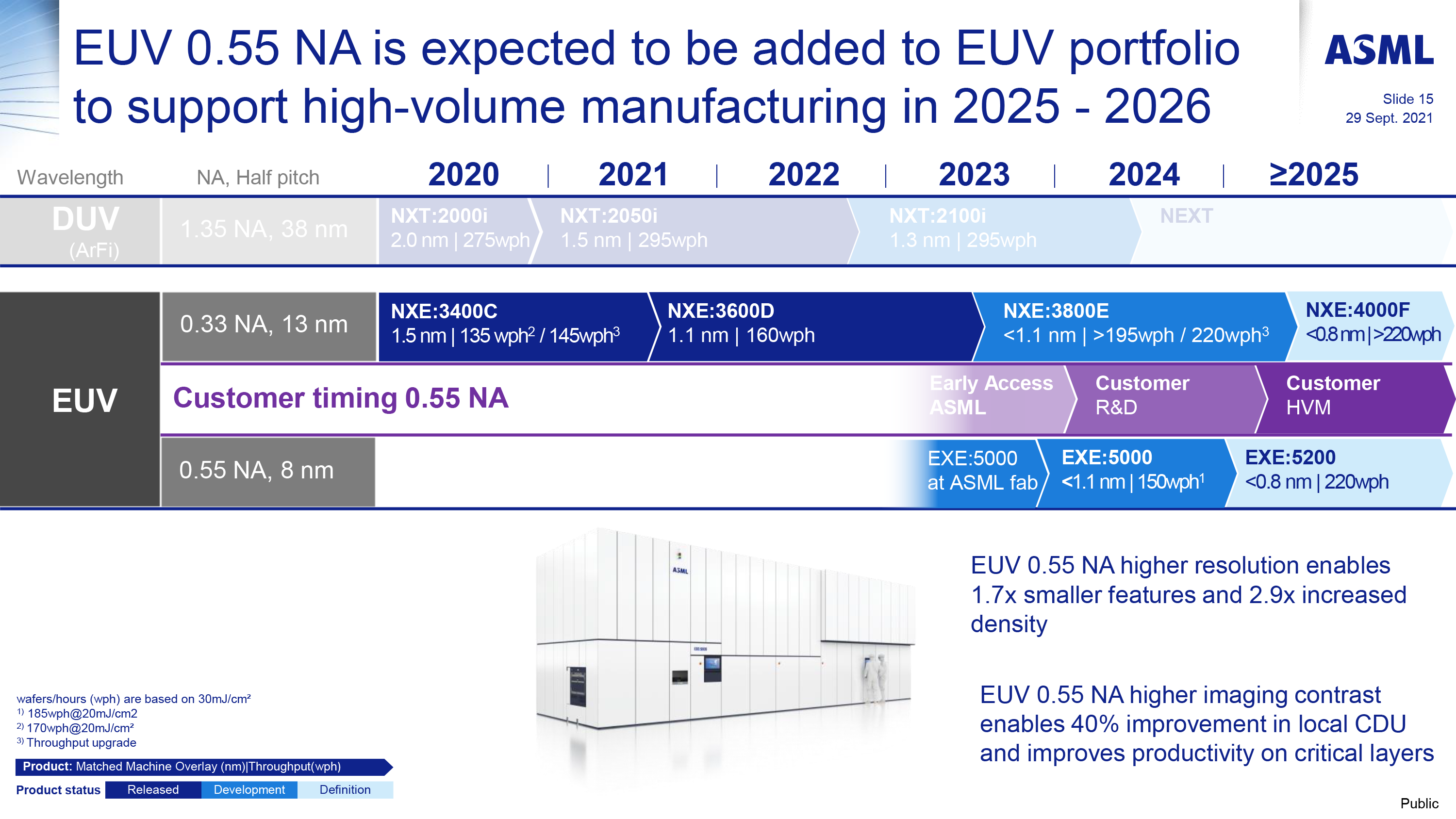
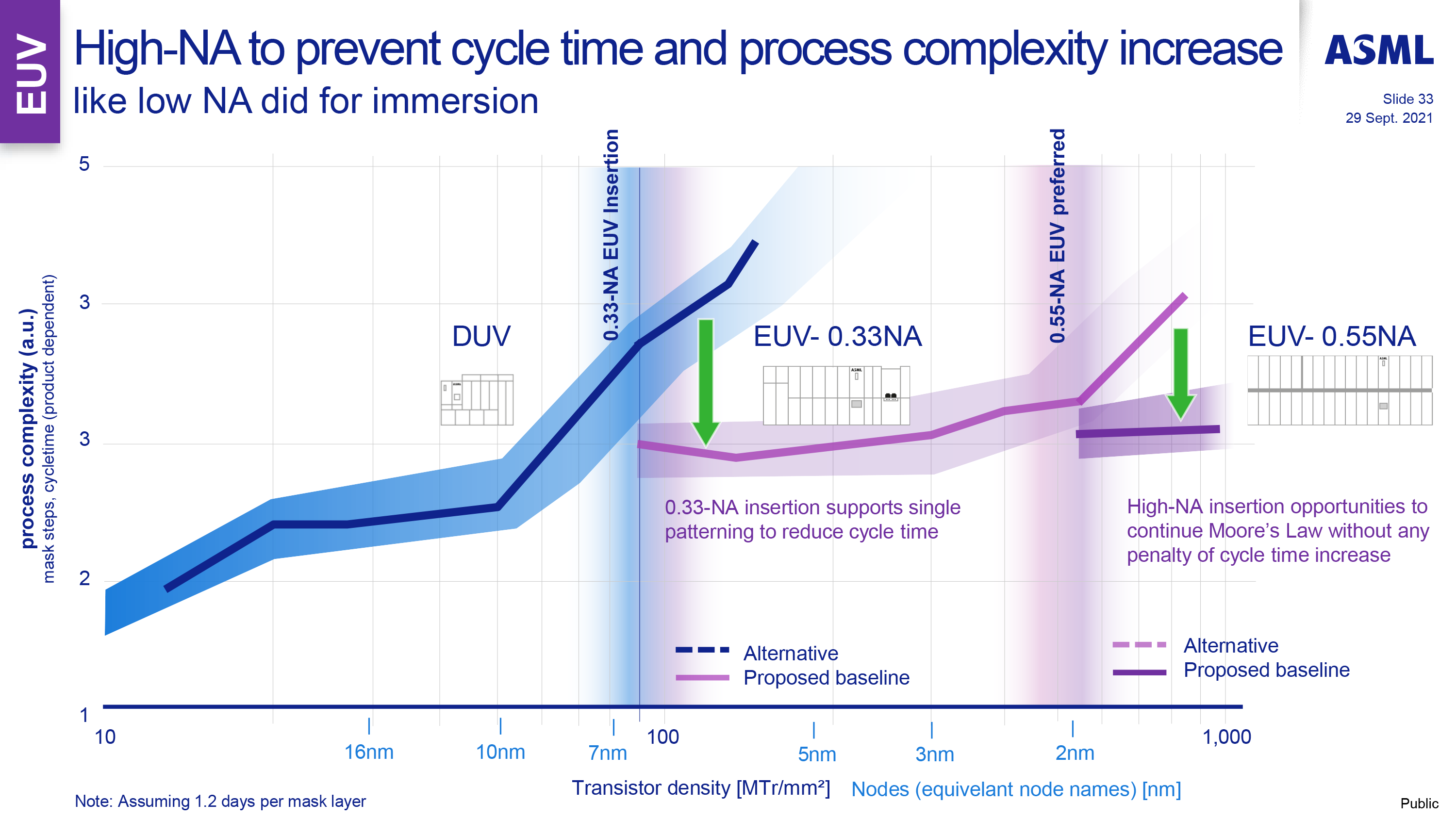
High-NA EUV litho machines are outfitted with a 0.55 NA (High-NA) lens that can achieve a resolution of 8nm, a major improvement over existing EUV tools — the existing 0.33 NA (Low-NA) lens offers a 13nm resolution. The resolution improvement will be crucial for post-2nm technologies requiring either Low-NA EUV double patterning or High-NA EUV single patterning. Each EUV High-NA scanner is expected to cost from $300 million to $400 million.
Intel will start installing the Twinscan EXE:5000 machine that can process 150 wafers per hour (at a dose of 30mJ/cm^2) with a <1.1nm matched-machine overlay performance. This machine will be used primarily to learn how to use High-NA EUV with Intel's 18A (18 angstroms, 1.8nm) process technology, but the real high-volume manufacturing (HVM) will commence using a post-18A node on ASML's Twinscan EXE:5200 machines. These machines will increase productivity to 220 wph and imaging performance to <0.8nm matched-machine overlay.
Intel wants to get back its fabrication technology leadership, and the company hopes to do so with 18A. With High-NA-enabled post-18A production nodes, Intel not only hopes to maintain power, performance, and area leadership but essentially establish its own standards when it comes to High-NA manufacturing. This could prove to be a strategic advantage over its rivals, much like TSMC's pathfinding work with the first Low-NA machines helped it establish and maintain a lead over Intel.
Get Tom's Hardware's best news and in-depth reviews, straight to your inbox.

Anton Shilov is a contributing writer at Tom’s Hardware. Over the past couple of decades, he has covered everything from CPUs and GPUs to supercomputers and from modern process technologies and latest fab tools to high-tech industry trends.
-
peachpuff ReplyThe two companies will begin assembling the machine shortly
Don't let intel near it...
-
HaninTH Does it come with auto renewing support contracts for the life of the device? What's the return policy on this sort of kit? Do they provide return shipping labels?Reply -
rluker5 I like how ASML compares the step from DUV to EUV to the step from EUV to high NA EUV.Reply
It probably won't be that big of an improvement, but it will still be one.
Intel had a lot of troubles getting to 10nm on DUV and old EUV will probably give TSMC the same kind of troubles if they try to reach high NA EUV nodes with old EUV. -
strobolt I'm a total noob when it comes to the chip manufacturing but wanted to ask that how is it possible to produce 1,8 nm process nodes with 8 nm resolution? Does this have something to do with how I've heard it being said that 1,8 nm nodes are not really 1,8 nm but it's more of an marketing tactic?Reply -
thestryker Reply
Volume of production wise it probably is that big, but in terms of allowing more density probably not.rluker5 said:I like how ASML compares the step from DUV to EUV to the step from EUV to high NA EUV.
It probably won't be that big of an improvement, but it will still be one.
I don't think they'll have the same level of problems in terms of getting it to work. They will have the same exact problem with regards to cost scaling though which isn't sustainable.rluker5 said:Intel had a lot of troubles getting to 10nm on DUV and old EUV will probably give TSMC the same kind of troubles if they try to reach high NA EUV nodes with old EUV.
Fabrication node names have been completely meaningless since Intel released 22nm, TSMC 16nm and Samsung 14nm as they all switched to FinFET transistors.strobolt said:I'm a total noob when it comes to the chip manufacturing but wanted to ask that how is it possible to produce 1,8 nm process nodes with 8 nm resolution? Does this have something to do with how I've heard it being said that 1,8 nm nodes are not really 1,8 nm but it's more of an marketing tactic? -
Eskimou Reply
You are correct that 1.8nm seems beyond a 8nm resolution. Rayleigh's equation tells us that the minimum CD is equal to a k1 factor times wavelength over numerical aperture. Theoretical k1 limit typically used is 0.25. So CD = 0.25 *(13.5nm/0.55) results in a CD a little over 6nm, 8nm is a fair assumption as it gives a little lee way since it's almost impossible to reach a perfect 0.25 factor.strobolt said:I'm a total noob when it comes to the chip manufacturing but wanted to ask that how is it possible to produce 1,8 nm process nodes with 8 nm resolution? Does this have something to do with how I've heard it being said that 1,8 nm nodes are not really 1,8 nm but it's more of an marketing tactic?
The industry has been producing sub theoretical for some time through the use of multiple exposure patterning and other "tricks" of the trade like self aligned double or quadruple patterning. While specific techniques are closely guarded secrets you can read about general techniques here: https://en.wikipedia.org/wiki/Multiple_patterning


