Next-generation 3D DRAM approaches reality as scientists achieve 120-layer stack using advanced deposition techniques
High-density 3D DRAM might be around the corner.

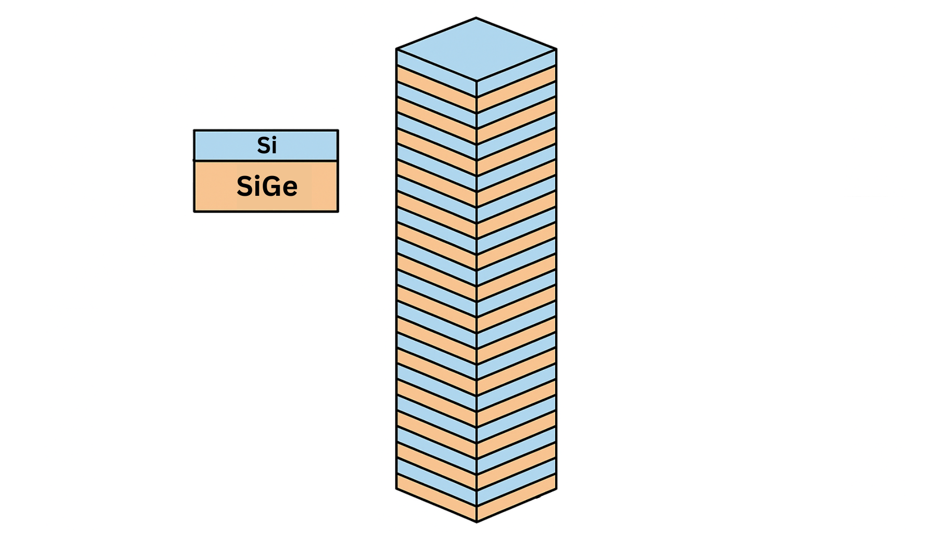
Imagine trying to build a tower out of hundreds of very thin, slightly different sheets of material, where each sheet wants to bend or warp on its own. That’s essentially what researchers at imec and Ghent University accomplished when they grew 120 alternating layers of silicon (Si) and silicon-germanium (SiGe) on a 300 mm wafer—a key step toward three-dimensional DRAM. At first glance, it sounds like stacking sheets of paper; in reality, it’s more like balancing a house of cards with materials that naturally want to pull apart.
The challenge starts with lattice mismatch. Silicon and silicon-germanium crystals have slightly different atomic spacings, so when stacked, the layers naturally want to stretch or compress. Think of it like trying to stack a deck of cards where every second card is slightly larger than the first—without careful alignment, the stack warps and topples. In semiconductor terms, these “topples” appear as misfit dislocations, tiny defects that can ruin a memory chip’s performance.
To solve this, the team carefully tuned the germanium content in the SiGe layers and experimented with adding carbon, which acts like a subtle glue that relieves stress. They also maintained extremely uniform temperatures during the deposition process, because even minor hot or cold spots in the reactor can lead to uneven growth.
Article continues below 
The process itself, using advanced epitaxial deposition techniques, is like painting with gases. Silane and germane—gases containing silicon and germanium—are broken down on the wafer surface, leaving behind precise, nanometer-thin layers. Controlling the thickness, composition, and uniformity of each layer is crucial; even a tiny deviation can propagate through the stack, magnifying defects.
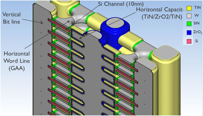
Now, why go through all this effort? In conventional DRAM, memory cells are laid out flat, limiting density. Stacking layers vertically—in 3D—allows for far more memory cells in the same footprint, improving storage capacity without making chips larger. Successfully creating 120 bilayers demonstrates that vertical scaling is achievable, bringing us closer to next-generation, high-density memory devices.
Think of each bilayer as a story in a skyscraper, if one floor is misaligned then the entire building becomes unstable. By controlling strain and keeping layers uniform, the researchers effectively built a nanoscale skyscraper of silicon and SiGe that could host thousands of memory cells per unit area.

The implications stretch beyond memory chips. Techniques for growing precise multi-layer structures can advance 3D transistors, stacked logic devices, and even quantum computing architectures, where controlling layer properties at the atomic level is critical. Samsung has already put 3D DRAM on its roadmap and even has a dedicated R&D facility for it.

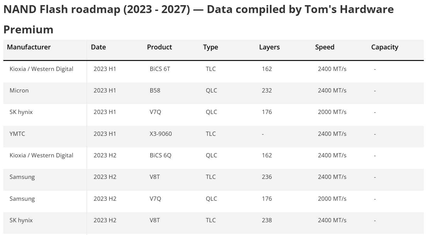
Want more? We've got an exclusive roadmap to the future of 3D NAND flash — only for subscribers of Tom's Hardware Premium.
Furthermore, the research aligns with ongoing efforts to develop Gate-All-Around Field-Effect Transistor (GAAFET) and Complementary FET (CFET) technologies. These advanced transistor architectures benefit from the precise control over material properties afforded by epitaxial growth techniques, enabling the fabrication of smaller, more powerful transistors that are crucial for the continued miniaturization of electronic devices.
In summary, this is not just stacking silicon as you might know; it’s engineering order from atomic tension, creating structures that nature itself would struggle to produce. For memory technology, like we say with every new breakthrough, it’s a milestone that could reshape how chips are designed, making them denser, faster, and more reliable than ever before.
Follow Tom's Hardware on Google News to get our up-to-date news, analysis, and reviews in your feeds. Make sure to click the Follow button.

Hassam Nasir is a die-hard hardware enthusiast with years of experience as a tech editor and writer, focusing on detailed CPU comparisons and general hardware news. When he’s not working, you’ll find him bending tubes for his ever-evolving custom water-loop gaming rig or benchmarking the latest CPUs and GPUs just for fun.
-
ekio If manufacturers do not virtually limit availability and access!Reply
Just like they did for Ram ans Storage these past 5 years where nothing improved on purpose……….. -
usertests From what I read, Samsung is planning to start with 16 layers. If we eventually see around 128 layers it could be for a ≥4 terabit die.Reply
There have been improvements, they are just subject to cyclical price swings that wipe out $/TB gains.ekio said:If manufacturers do not virtually limit availability and access!
Just like they did for Ram ans Storage these past 5 years where nothing improved on purpose………..
In RAM specifically, we saw 24 Gb DRAM dies used in 48 GB (consumer) DIMMs, and now 32 Gb in 64 GB DIMMs that were launched earlier this year.
As long as 3D DRAM drives down cost-per-bit and starts replacing planar DRAM, it will eventually make it to consumers. That's unlike the TSV-stacked DRAM used in current 256/512 GB server modules which achieves additional density with a cost multiplier. -
chaz_music It appears that they are also trying to use sideways thermal paths to get the heat out, which is why I see this going to ECC to detect thermally induced errors and bit flips. And I would be cautious for the first generation of this as the thermal strain between the Si and SiGe layers could cause these to have a short life span. Especially in high thermal transient conditions such as fast RAM loading and accessing for AI, simulations, CAD, and other large dataset and matrices uses. If an application heats the chip stack up fast and then lets it cool fast, that strain can induce cracks and lattice damage through thermal cycling.Reply
When they figure out how to use SiC as the primary material, this will get very exciting. Much faster material with a large bandgap energy, and a great thermal conductor. This should get us into the THz range for switching.
And just think: visible light is in the 700THz region, so no need to to add RGB LED's to a PC. The traces will glow by themselves with visible light, but we wouldn't want UV though. I would expect us to be using optical signalling for data by then anyway.
But they could make direct RF light bulbs ... -
abufrejoval Sound like a fairly large corner to me, like a decade, or two, if everything goes right or works at all.Reply
That's also where IMEC tends to operate.
So far that's only about uniform deposition of layers and managing misfits, that tend to accumulate towards the wafer edge. They aren't etching structures yet, nor managing defects 120 layers deep: this sounds as if HBMs were easy in comparison and there you can test the chips (not wafers) you plan to stack instead of doing 120 layers of a wafer, only to find that things had gone fundamentally wrong in layer 13 already.
Then there is the heat aspect: unlike the non-volatile memristor stacks HP hallucinated 20-10 years ago, DRAM needs refreshes just to maintain state and power to operate, which implies heat. And staggering those refreshes in such a manner that you don't have 120 vertical rows light up at once, may be extra tough to do.
I remember reading papers years ago, which were all about ways to just cool stacked DRAM enough via "climate control TSVs" to avoid self-ignition.
I also wonder, what the actual density would be, since they still need to account for capacitance: since they can't very likely use the z (height) axis for the deep trenches normally required to achieve significant capacitance to hold a charge, either x or y need to yield, which trades depth with resolution and makes limited sense to me.
So no, while 'around the corner' isn't a well defined time period, I see this as the typical IMEC exploratory work, nothing I'd encounter as a finished product, next time I turn a corner to meet a computer shop. -
JRStern As others have said it all comes down to one word: heat.Reply
Maybe you can stack them with big, thick copper layers, even if that limits the stack to just some modest number, 4 or 8 or 42, I don't know, and whatever electrical insulation they also need, or some magic ceramic that is electrically insulating and conducts heat well, ...
... or just stack them like HBM, what the heck. -
usertests Reply
Samsung's plan is 16 layers for their first generation, sometime in the early 2030s. So maybe 6-8 years from now.abufrejoval said:So no, while 'around the corner' isn't a well defined time period, I see this as the typical IMEC exploratory work, nothing I'd encounter as a finished product, next time I turn a corner to meet a computer shop.
https://www.tomshardware.com/pc-components/ram/samsung-reveals-16-layer-3d-dram-plans-with-vct-dram-as-a-stepping-stone-imw-2024-details-the-future-of-compact-higher-density-ram
Before that, they will switch over to VCTs. We have 32 Gb DRAM dies now, and they will definitely be producing 48 Gb, maybe up to 64-96 Gb before any 3D DRAM lands.
TSV DRAM is already a thing. That's how you get a 512 GB DDR5 memory module for servers. It's a good tool but it doesn't make memory cheaper like 3D DRAM will.JRStern said:... or just stack them like HBM, what the heck. -
micheal_15 2027. Samsung announces new 4TB ram chips. A single Dimm can now have 32TB of memory. 4 stacks gives you 128 TERABYTES of memory.Reply
This just manages to meet the minimum spec for Windows 12. -
DS426 From an economics and business risk (specically supply chain risk) standpoint, is relying on Germanium a good idea? Doesn't China supply the majority of this rare resource? Hopefully 3D DRAM can move forward without necessarily relying on it.Reply -
abufrejoval Reply
Ok, so it definitely looks like they'll use x or y to create the capacitors instead of digging tinier and deeper holes.usertests said:Samsung's plan is 16 layers for their first generation, sometime in the early 2030s. So maybe 6-8 years from now.
https://www.tomshardware.com/pc-components/ram/samsung-reveals-16-layer-3d-dram-plans-with-vct-dram-as-a-stepping-stone-imw-2024-details-the-future-of-compact-higher-density-ram
Before that, they will switch over to VCTs. We have 32 Gb DRAM dies now, and they will definitely be producing 48 Gb, maybe up to 64-96 Gb before any 3D DRAM lands.
TSV DRAM is already a thing. That's how you get a 512 GB DDR5 memory module for servers. It's a good tool but it doesn't make memory cheaper like 3D DRAM will.
Since those got to be really hard to do, flipping RAM to the side to create them via deposition seems the original driver and the extra layers are mostly to compensate the loss of square gains, right?
And then 120 layers are really about exploring the frontiers, while layer counts will follow what happened with flash.
I guess Row Hammer and heat will call for complex compensation measures, but there is no real reason why you couldn't just add the logic layers for that in between.
What remains challenging is obviously the precision control issues and that this seems to lengthen fab production cycles for every additional layer: there is no shortcutting a sequential process, which doesn't affect stacked or fused dies nearly as much.
Good thing these aren't CPUs... although the potential for PIM becomes much bigger...