ASML ships groundbreaking new chipmaking tool to Intel — High-NA lithography tool needed for next-gen process nodes could cost ~$400 million
An industry first.

ASML on Thursday announced that it had begun shipping the industry's first extreme ultraviolet (EUV) lithography tool with a 0.55 numerical aperture (High-NA) to Intel. The initial High-NA machine will be used to learn how it works on Intel's 18A (18 angstroms, 1.8nm-class) fabrication process, which promises to provide the CPU giant a lead over its rivals TSMC and Samsung.
"We are shipping the first High NA system and announced this in a social media post today," a spokesperson for ASML said. "It goes to Intel as planned and announced earlier."
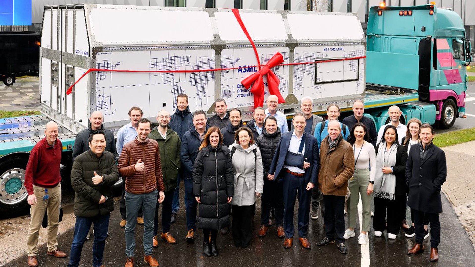
As announced in September, ASML this week began to (literally) ship its High-NA EUV lithography tool to Intel. The unit will be shipped from Veldhoven, the Netherlands, to Intel's site near Hillsboro, Oregon, and will be installed there over the next few months. The machine is so big that it takes 13 huge containers and 250 crates to ship it. It is believed that each High-NA EUV scanner costs somewhere around $300 to $400 million.
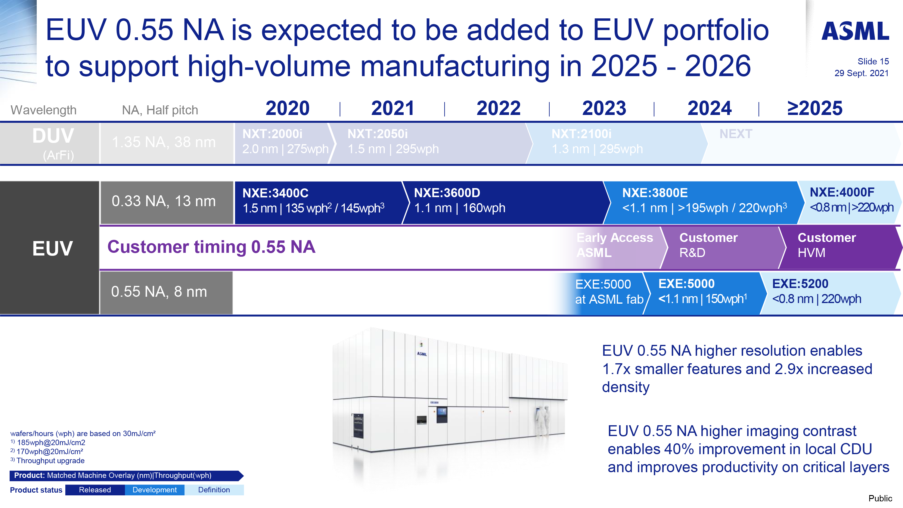
The High-NA EUV tool that ASML ships is pilot Twinscan EXE:5000 machine which Intel acquired in 2018. This unit will be used by Intel to better learn high High-NA EUV tools work on its 18A process technology and gain valuable experience before the company will deploy commercial-grade Twinscan EXE:5200 machines for high-volume chip manufacturing beginning in 2025 using a post-18A production node.
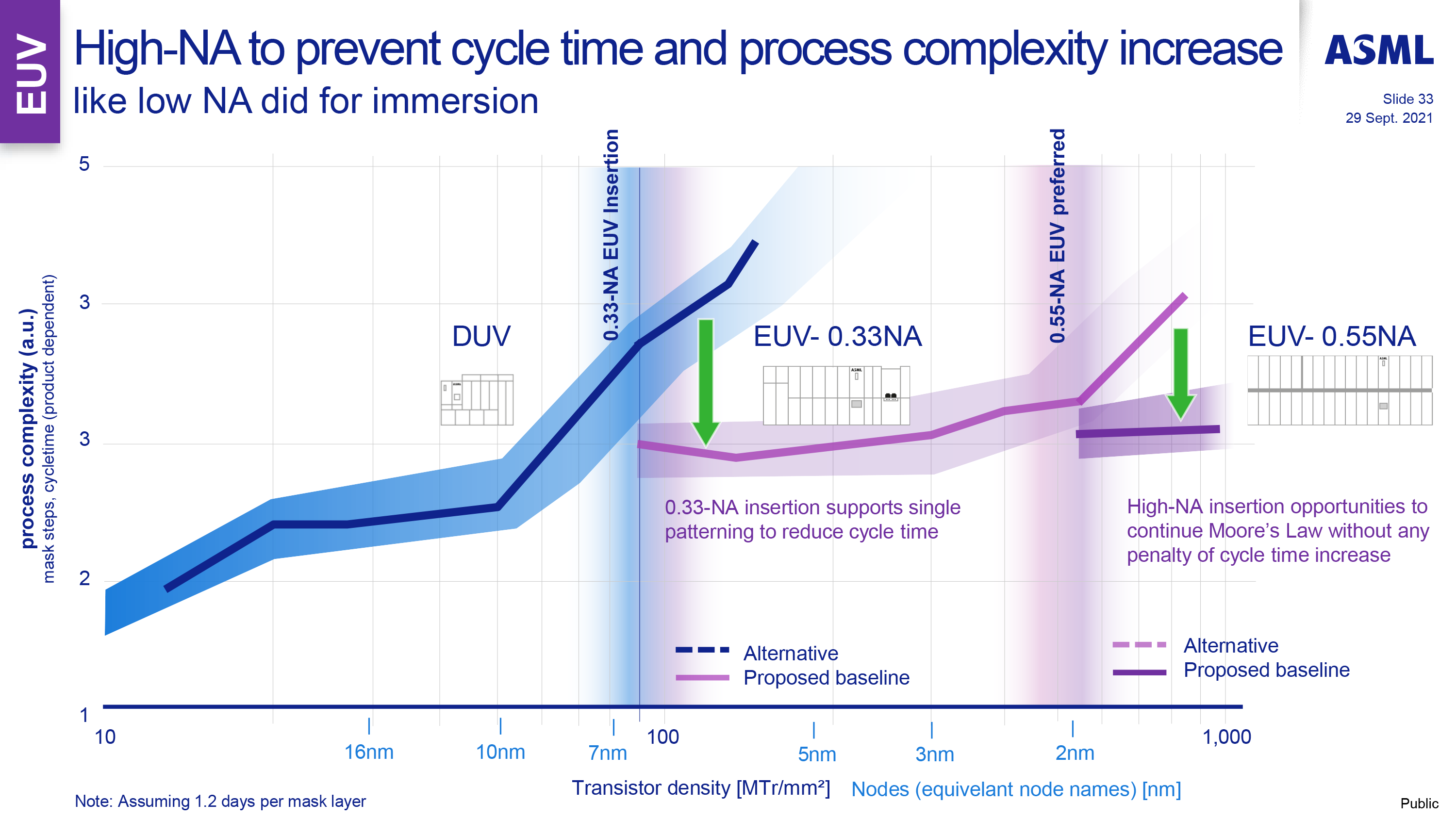
High-NA EUV lithography tools equipped with a 0.55 NA (High-NA) lens can achieve a resolution of 8nm, a notable advancement over standard EUV tools with a 0.33 NA (Low-NA) lens that offer a 13nm resolution. High-NA technology are projected to play a crucial role for post 2nm-class process technologies that will either need to use Low-NA EUV double patterning or High-NA EUV single-patterning.
Since High-NA lithography tools have a number of differences with Low-NA litho machines that will require a lot of infrastructural changes, deploying a Twinscan EXE quarters ahead of its rivals could be a huge advantage for Intel. On the one hand, Intel will have plenty of time to adjust its post-18A process technologies. On the other hand, the company will adjust High-NA infrastructure for itself, which will give it another advantage over its competitors.
Get Tom's Hardware's best news and in-depth reviews, straight to your inbox.

Anton Shilov is a contributing writer at Tom’s Hardware. Over the past couple of decades, he has covered everything from CPUs and GPUs to supercomputers and from modern process technologies and latest fab tools to high-tech industry trends.
-
rtoaht It’s amazing how so many people in tech forums don’t believe that Intel will regain the process technology leadership. The same company that kept the process leadership for many decades until recently.Reply
Most people know about their 10nm execution issues and forget or don’t know that TSMC had similar issues during FinFET transition and more recently with 3nm.
Time will tell what will happen in the future, but I wouldn’t just casually count them out. They might very well retake the leadership in a year or so. -
thestryker It's going to be interesting to see how Intel approaches High-NA and I'm hoping someone gets to do some interviews or they do some media pieces on it. I'm assuming that with the pilot EXE:5000 they're going to be predominantly putting it through its paces on existing nodes before moving on to ones beyond 18A.Reply
The main question I have is whether or not the EXE:5200s get installed early enough to be leveraged to optimize existing nodes or if they'll be used for what's next. If Intel wasn't trying to make IFS a real player I'd say future node, but these machines have the potential to limit multipatterning and have increased throughput. -
Rob1C While Intel may receive their machine first, for research, it is IBM and partners that will be making production chips first with their soon-to-arrive machine (same one):Reply
https://siliconangle.com/2023/12/11/new-york-state-ibm-micron-others-partner-cutting-edge-10b-chip-research-lab/https://research.ibm.com/blog/high-na-euv-lithography-albanyhttps://research.ibm.com/blog/2-nm-chip -
thestryker Reply
That says they're breaking ground 2024 and they're getting EXE:5200 which won't be shipping until some time next year (for the first batch which IBM may or may not be part of). The one being cited in this article is the pilot High-NA machine which is the EXE:5000 and Intel will have it installed and operating (unless something goes very wrong) well before anyone else has anything shipping.Rob1C said:While Intel may receive their machine first, for research, it is IBM and partners that will be making production chips first with their soon-to-arrive machine (same one):
https://siliconangle.com/2023/12/11/new-york-state-ibm-micron-others-partner-cutting-edge-10b-chip-research-lab/https://research.ibm.com/blog/high-na-euv-lithography-albanyhttps://research.ibm.com/blog/2-nm-chip
Now IBM's acquisition of a High-NA machine is probably the most important for the industry as a whole given how good their node research has been. Many leading edge nodes were either designed by or use research done by IBM.


