Ex-Intel CEO Pat Gelsinger gives Japan's new leading-edge chipmaker advice, says Rapidus needs unique tech to compete with TSMC
What could this possibly be?

Japan's Rapidus is gearing up to start rivalling for advanced TSMC customers with its 2nm-class process technology sometime in 2027, with some secret sauce involving advanced packaging at the same facility, thus speeding up the production cycle. However, Pat Gelsinger, a former Intel chief executive, says that Rapidus should offer something beyond just streamlined production, something special, according to the Japan Times.
"We applaud the efforts of Japan to bring Rapidus to the market," Gelsinger said at a press conference in Tokyo, responding to a question about the potential of Rapidus, as per Japan Times. "However, we would also say that Rapidus needs some fundamental differentiating technologies, because if they are trying to catch up with a well-executing TSMC without some leap-ahead capabilities, we think that is a very hard road."
One exclusive feature that Rapidus intends to offer compared to other major producers like Samsung, Intel, and TSMC is fully automated packaging integrated within the same site as wafer fabrication, which could shorten production timelines. However, this capability will not be active immediately, since the initial phase of the fab will only include wafer pilot manufacturing without packaging services.
Rapidus is about to start test production of wafers using its 2nm process technology, which relies on gate-all-around transistors and aims to begin high-volume semiconductor manufacturing using this node by 2027. The company aims to deliver the first sample wafers by July and will provide early clients with design tools to help them build prototypes.
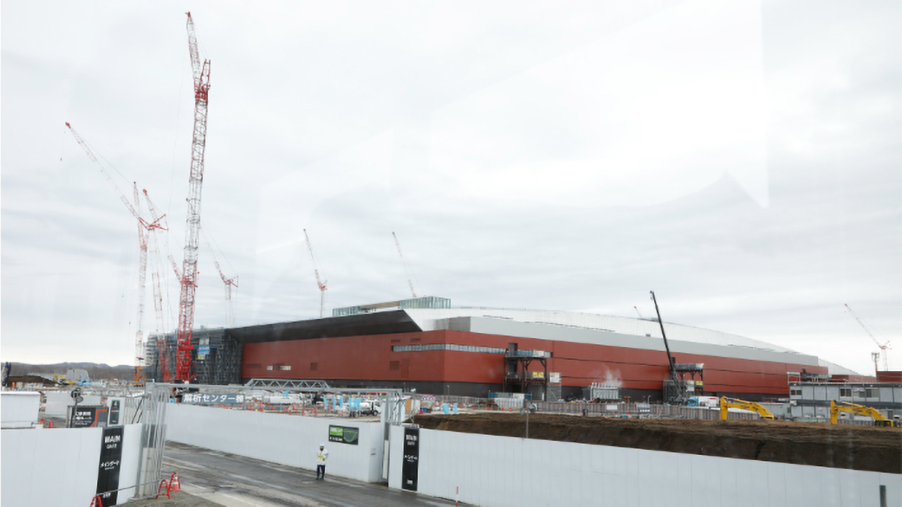
Rapidys has set up ASML's EUV and DUV lithography machines inside its Innovative Integration for Manufacturing facility in Chitose, Hokkaido. These systems were installed late last year, and the project has likely achieved the early operational milestone needed to start pilot runs, although neither Rapidus nor ASML has announced the first light-on-wafer milestone.
In addition, Rapidus is establishing a research center, called Rapidus Chiplet Solutions, at Seiko Epson's Chitose location, adjacent to the central facility. Preparations have been underway since October 2024, and equipment installation is scheduled to begin this month. The site will focus on scaling up post-fabrication work, including the development of redistribution layers, 3D packaging processes, assembly design tools, and methods for testing known-good dies (i.e., HBM modules).
Follow Tom's Hardware on Google News to get our up-to-date news, analysis, and reviews in your feeds. Make sure to click the Follow button.
Get Tom's Hardware's best news and in-depth reviews, straight to your inbox.

Anton Shilov is a contributing writer at Tom’s Hardware. Over the past couple of decades, he has covered everything from CPUs and GPUs to supercomputers and from modern process technologies and latest fab tools to high-tech industry trends.
-
wussupi83 Does this fab really have to be a world leader to be a success? I would think a fab would still be a useful asset to Japan. I guess we will see in 5-10 years what happens to all of these fab projects.Reply -
bit_user Reply
The reason they seem to be pumping so much money into it seems to be that they want a manufacturing capability that's truly competitive. I assume that's because, if other countries block Japanese companies' access to their fabs, Japan doesn't want to be left in a situation where all of its products (both chips and products requiring advanced semiconductors, like self-driving cars, etc.) aren't competitive because they're limited to using older tech.wussupi83 said:Does this fab really have to be a world leader to be a success?
Sure, there are plenty of chips that don't need to be on the latest node, but Japan already has some older fabs and if they ever want Rapidus to have a chance at being self-sustaining, then they have to get to a point where people are willing to pay high prices for the wafers they're producing. I sort of doubt the government wants it to be an endless money pit.wussupi83 said:I would think a fab would still be a useful asset to Japan. -
Notton Gelsinger is correct.Reply
2nm, but no CoWoS, die stacking, backside power delivery, GAAFET etc. -
bit_user Reply
Um, but it will have GAA!Notton said:Gelsinger is correct.
2nm, but no CoWoS, die stacking, backside power delivery, GAAFET etc. -
Notton Reply
oh, it does? did not know that.bit_user said:Um, but it will have GAA!
That'll put them on the same level as Samsung, I guess. -
bit_user Reply
That's what the article says. It's written out, not abbreviated.Notton said:oh, it does? did not know that.