TSMC claims 4.2X efficiency gain over a decade from N7 to A14 fabrication process
Slowly but surely.

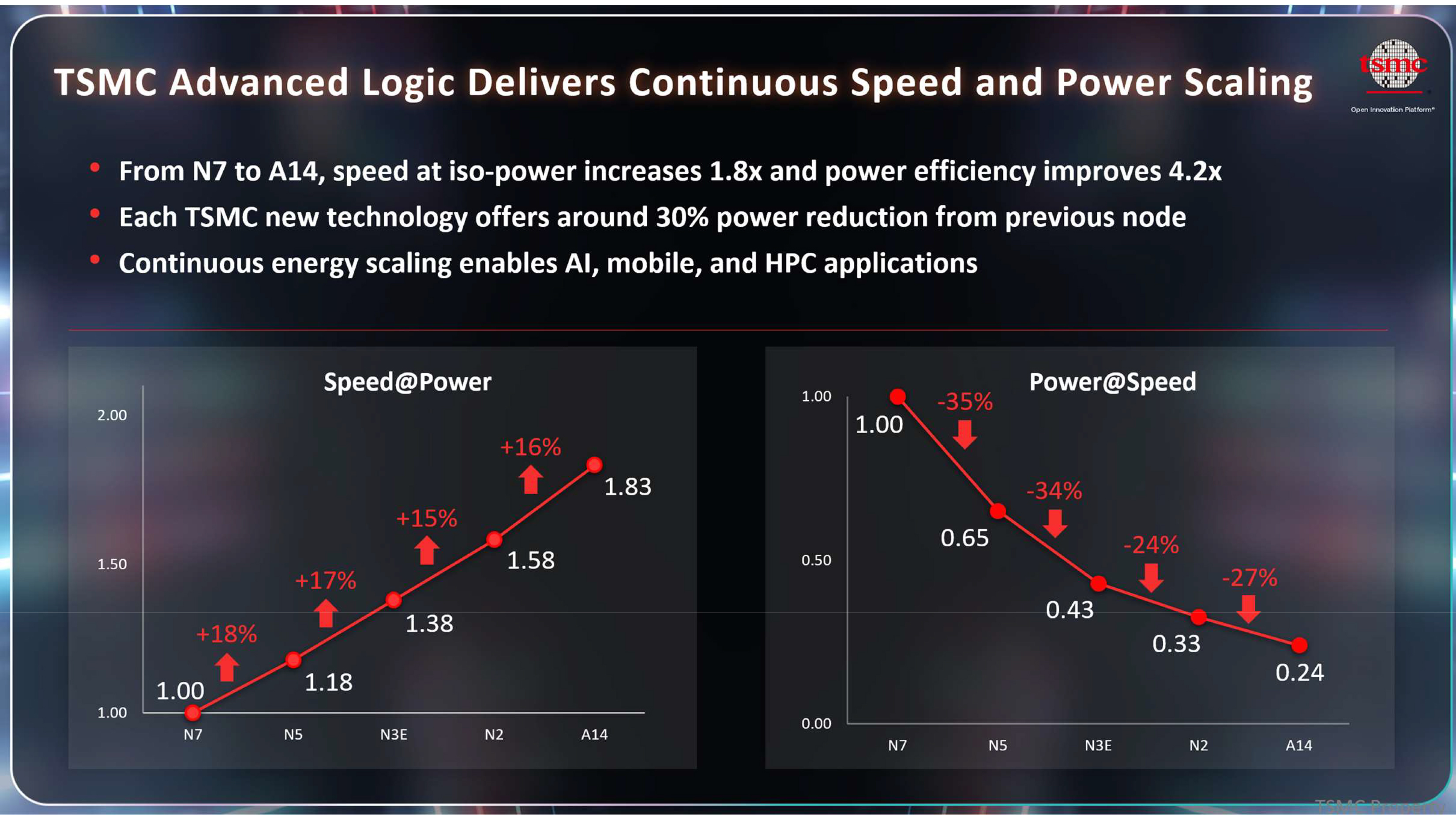
A slide that TSMC has demonstrated at its European OIP forum clarifies the advantages that its A14 (1.4nm-class, front side power delivery) fabrication process, due in 2028, will offer compared to the direct predecessor. As it turns out, A14 will offer 16% more performance at the same power and complexity, and 27% lower power at the same clocks and complexity compared to N2 (2nm-class, front side power delivery). Yet, to extract the full potential of next-generation manufacturing technologies, chip designers might need to use smarter electronic design automation (EDA) tools.

When foundries announce new process technologies, they usually disclose a range of characteristics that show the relative difference between generations. As development of the production node proceeds, chipmakers tend to get more data about its capabilities and therefore clarify its characteristics over time. This is precisely what happened to TSMC's A14. Previously, the company said that compared to N2, it will offer from 10% to 15% higher performance at the same power and transistor count, 25% to 30% lower power at the same clocks and complexity, and about 20% higher 'mixed chip' transistor density. As it turns out from the slide, the new node will offer a bit higher performance than anticipated, but will remain in the mid-point of what was predicted in terms of power consumption.

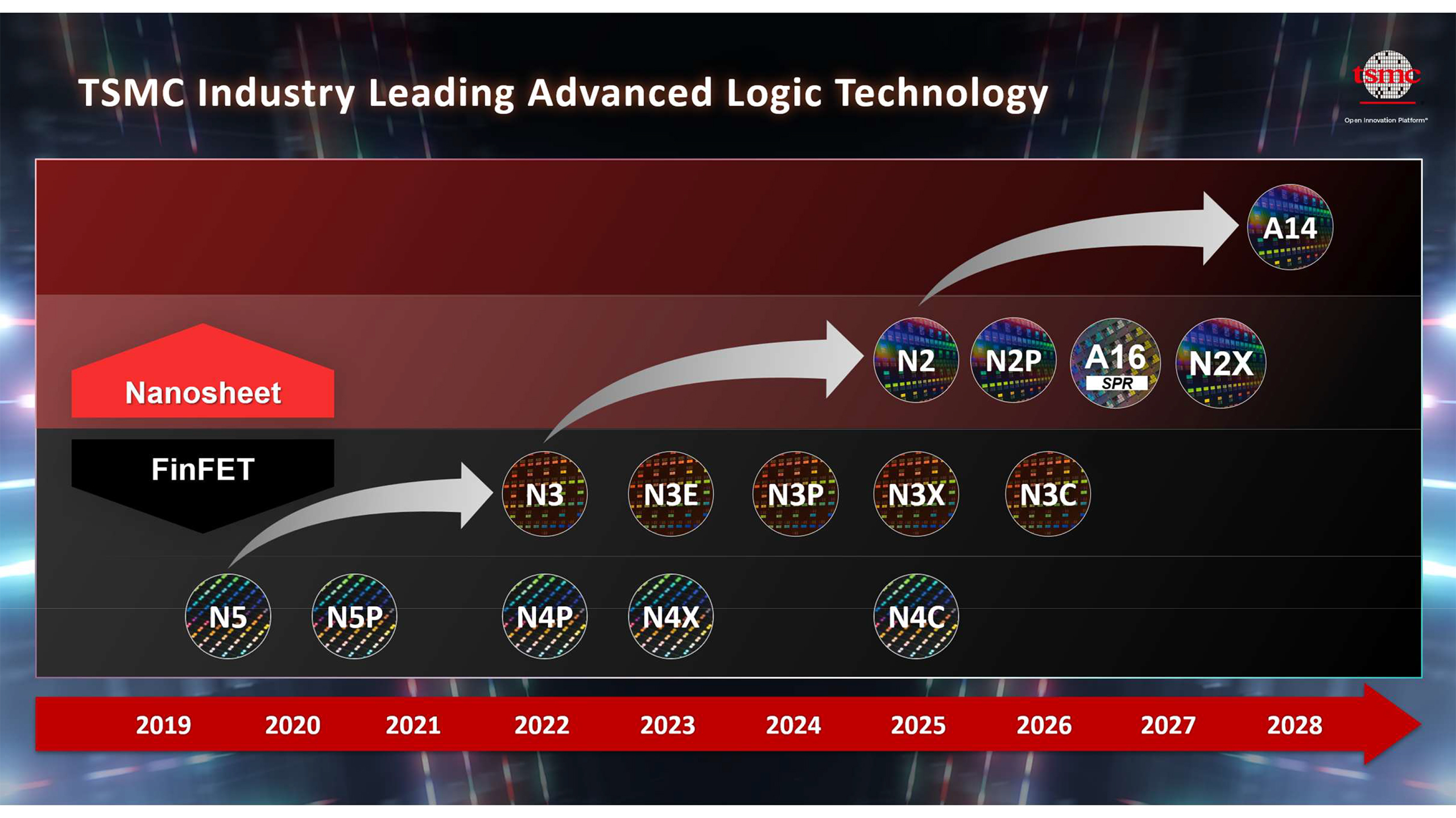
TSMC demonstrated the slide to show the scalability of its process technologies, as part of a broader effort to say that Moore's Law is very much alive, despite slowing and facing severe challenges. Meanwhile, the slide lists only major mainstream nodes and omits N3B (which was used primarily by Apple and Intel) and inter-node updates such as N3P and N2P. While the mention of N3X, N2X, and A16 makes sense, since these fabrication technologies are aimed at particular applications, the lack of inter-node updates somewhat blurs their importance and the advancements they tend to bring, highlighting the increments made over the years.
According to the slide, moving from N7 (a 2018 node) to A14 (a 2028 node) increases performance at the same power level by 1.83X and improves power efficiency by 4.2X, which looks impressive. Still, there is a decade between these technologies. TSMC also states that each new major process generation delivers about 30% power reduction compared to the previous node. In contrast, performance improvements are limited to 15% - 18% for major nodes, which somewhat highlights that power consumption was more of a focus for TSMC when designing these fabrication technologies.
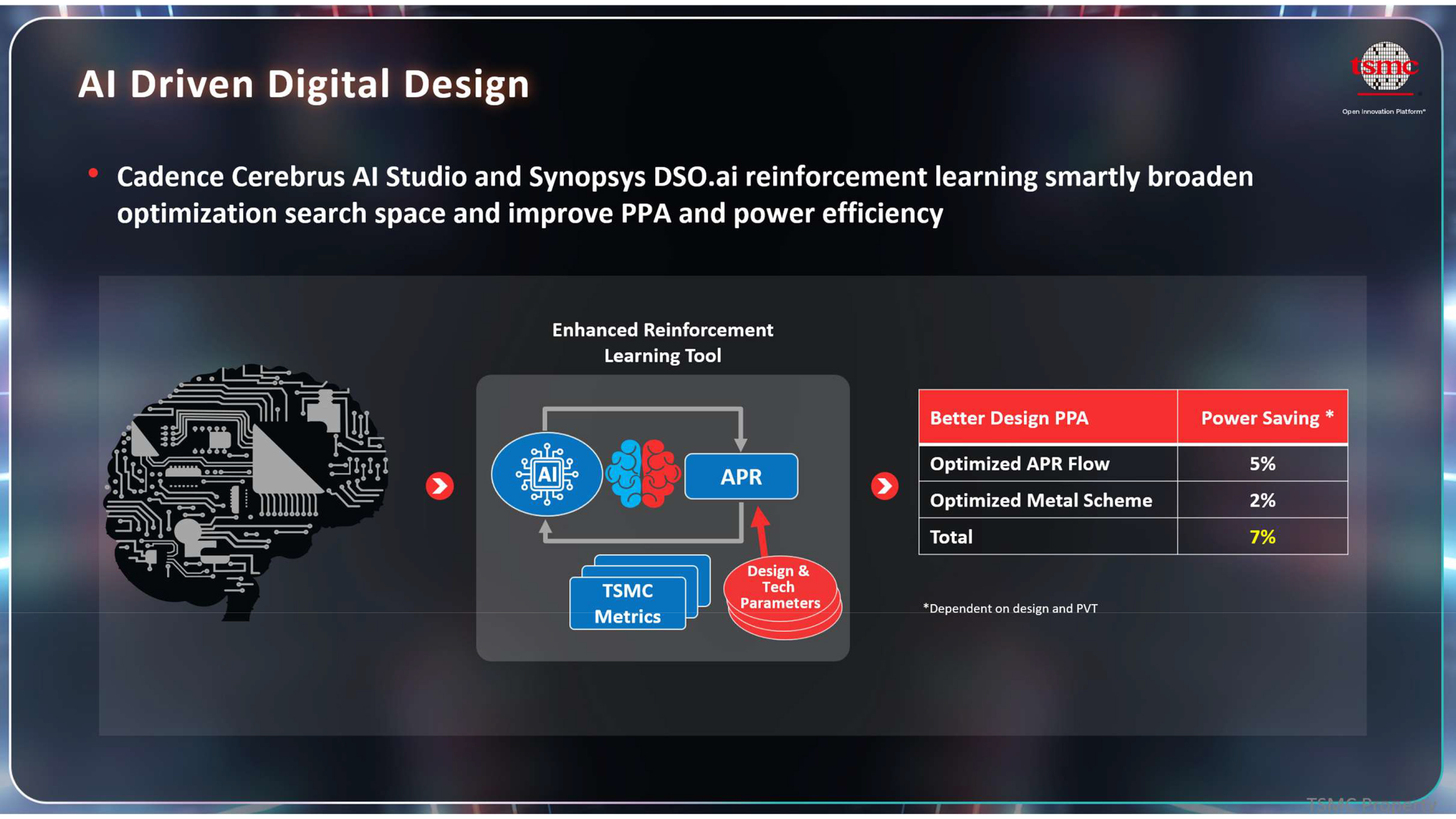
Interestingly, there are other ways to enhance the power efficiency of designs beyond what TSMC's nodes offer. For example, chip designers can use AI-enhanced Cadence Cerebrus AI Studio and Synopsys DSO.ai automated place-and-route (APR) EDA tools that use reinforcement learning to explore a broader optimization space across fabrication technologies and layout, and automatically tune design parameters and floorplan to improve performance, power, and area (PPA).

According to the slide, this approach delivers a 5% power saving from optimized APR flow, an additional 2% improvement from optimized metal scheme, and a total power saving of 7%, which is comparable to what TSMC can achieve from inter-node improvements. Of course, such promises should be taken with a grain of salt, as not all designs can be optimized to this extent. Still, no one can deny that EDA tools, in general, and smarter APR tools, in particular, are playing a bigger role in achieving higher performance at lower power with modern fabrication technologies.

Follow Tom's Hardware on Google News, or add us as a preferred source, to get our latest news, analysis, & reviews in your feeds.
Get Tom's Hardware's best news and in-depth reviews, straight to your inbox.

Anton Shilov is a contributing writer at Tom’s Hardware. Over the past couple of decades, he has covered everything from CPUs and GPUs to supercomputers and from modern process technologies and latest fab tools to high-tech industry trends.
