
Google TPUs garner attention as AI chip alternative, but are only a minor threat to Nvidia's dominance — Alphabet's biggest challenge is widespread adoption

Nvidia has broken its silence following reports that Meta is in advanced discussions to spend billions of dollars on Google’s custom Tensor Processing Units (TPUs), a move that would mark a rare shift in the company's AI infrastructure strategy. Nvidia, which saw its stock dip last week as Alphabet’s rose, issued a pointed statement in response on Tuesday.
“We’re delighted by Google’s success — they’ve made great advances in AI and we continue to supply to Google,” Nvidia wrote. “NVIDIA is a generation ahead of the industry — it’s the only platform that runs every AI model and does it everywhere computing is done. NVIDIA offers greater performance, versatility, and fungibility than ASICs, which are designed for specific AI frameworks or functions.”
The response highlights Nvidia’s awareness of what’s at stake. While Meta’s reported plan involves an initial rental phase and phased purchases starting in 2027, any serious pivot away from Nvidia hardware would reverberate throughout the AI ecosystem. Google’s TPU architecture, once used solely in-house, is now part of an aggressive bid to capture hyperscaler business from Nvidia’s dominant platform.
Article continues belowWe’re delighted by Google’s success — they’ve made great advances in AI and we continue to supply to Google.NVIDIA is a generation ahead of the industry — it’s the only platform that runs every AI model and does it everywhere computing is done.NVIDIA offers greater…November 25, 2025
ASIC acceleration vs GPU versatility
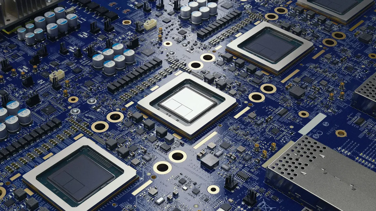
Google’s TPUs are application-specific chips, tuned for high-throughput matrix operations central to large language model training and inference. The current-generation TPU v5p features 95 gigabytes of HBM3 memory and a bfloat16 peak throughput of more than 450 TFLOPS per chip. TPU v5p pods can contain nearly 9,000 chips and are designed to scale efficiently inside Google Cloud’s infrastructure.
Crucially, Google owns the TPU architecture, instruction set, and software stack. Broadcom acts as Google's silicon implementation partner, converting Google’s architecture into a manufacturable ASIC layout. Broadcom also supplies high-speed SerDes, power management, packaging, and handles post-fabrication testing. Chip fabrication is performed by TSMC itself.
By contrast, Nvidia’s Hopper-based H100 GPU includes 80 billion transistors, 80 gigabytes of HBM3 memory, and delivers up to 4 PFLOPS of AI performance using FP8 precision. Its successor, the Blackwell-based GB200, increases HBM capacity to 192 gigabytes and peak throughput to around 20 PFLOPS. It’s also designed to work seamlessly in tandem with Grace CPUs in hybrid configurations, expanding Nvidia’s presence in both the cloud and emerging local compute nodes.

TPUs are programmed via Google’s XLA compiler stack, which serves as the backend for frameworks like JAX and TensorFlow. While the XLA-based approach offers performance portability across CPU, GPU, and TPU targets, it typically requires model developers to adopt specific libraries and compilation patterns tailored to Google’s runtime environment.
By contrast, Nvidia’s stack is broader and more deeply embedded in industry workflows. CUDA, cuDNN, TensorRT, and related developer tools form the default substrate for large-scale AI development and deployment. This tooling spans model optimization, distributed training, mixed-precision scheduling, and low-latency inference, all backed by a mature ecosystem of frameworks, pretrained models, and commercial support.
As a result, moving from CUDA to XLA is no trivial task. Developers must rewrite or re-tune code, manage different performance bottlenecks, and in some cases adopt entirely new frameworks. Meta has internal JAX development and is better positioned than most to experiment, but friction remains a gating factor for wider TPU adoption.
Second-source resilience
According to Reuters, some Google Cloud executives believe the Meta deal could generate revenue equal to as much as 10% of Nvidia’s current annual data center business. That is, of course, a speculative figure, but Google has already committed to delivering as many as one million TPUs to Anthropic and is pushing its XLA and JAX stack hard among AI startups looking for alternatives to CUDA.
Still, Google’s chips are single-purpose. TPUs do one thing and do it well, but with limits. They’re not suited for HPC simulations, general-purpose scientific computing, or any workload that requires flexible execution models or broad kernel support. TPU workloads run only in Google Cloud, while Nvidia chips run across clouds, on-prem systems, local workstations, and edge devices.
That flexibility is pretty central to Nvidia’s case. Hyperscalers like Meta are not new to custom silicon; AWS developed Trainium, Microsoft has Maia, and Google’s own TPU efforts date back nearly a decade. What’s new is the suggestion that another hyperscaler might shift some training off of Nvidia’s platform. Even if only partial, it highlights a desire for second-source resilience and bargaining power.
Grace Blackwell strengthens Nvidia’s position
Nvidia’s Grace Blackwell architecture will serve to make that kind of migration harder. By coupling Blackwell GPUs with Grace CPUs over a high-speed interconnect, Nvidia enables unified memory access and simplified training and inference workflows. Developers can train on GPU clusters in the cloud and serve models at the edge or in enterprise environments without changing code or retraining.
At the same time, Nvidia is moving deeper into vertical markets where TPUs don’t compete. It has partnerships across automotive, robotics, manufacturing, and retail. From Jetson edge modules to DGX supercomputers, Nvidia is positioning its stack as the default execution environment for AI inference everywhere, not just for training large models.
By exploring alternatives now, Meta potentially gains leverage in future hardware negotiations and insurance against vendor lock-in. Even if Google’s TPUs don’t replace H100s wholesale — which they likely won't — they could take on selected inference tasks or serve as overflow capacity in peak cycles, especially if the economics are favorable.
At this stage, Meta’s TPU adoption looks like little more than minor diversification. Nvidia continues to power the largest and most visible AI workloads in the industry. The company’s combination of software tooling, developer lock-in, and general-purpose capability gives it a lead that TPUs can’t erase overnight.
Google’s biggest challenge in all of this is going to be gaining ground from Nvidia. Meta’s participation would give TPUs credibility beyond Google Cloud and Anthropic, but scale is only part of the equation. Whether TPUs can meet the needs of complex, evolving AI workflows outside of a tightly controlled environment — and whether more hyperscalers are willing to put their faith in a platform that lives largely within one company’s walled garden — still remains to be seen.
