Nvidia Reveals Hopper H100 GPU With 80 Billion Transistors

Nvidia Hopper H100 GPU and DGX systems
(Image credit: Nvidia)

Today, at its GPU Technology Conference (GTC), Nvidia revealed details of its Hopper architecture and the Nvidia H100 GPU. We've known Nvidia has been working on next-generation GPUs for some time, but now we have some concrete specs. The Hopper architecture and H100 GPU are not to be confused with Ada, the consumer-focused architecture that will power future GeForce cards. Nvidia hasn't revealed any details on Ada yet, and Hopper H100 will supersede the Ampere A100, which itself replaced the Volta V100. These are all datacenter parts, and with steeper competition from the likes of AMD's Instinct MI250/250X and the newly announced Instinct MI210, Nvidia is looking to retake the lead in HPC.

As you'd expect given its legacy, H100 was designed for supercomputers with a focus on AI capabilities. It includes numerous updates and upgrades compared to the current A100, all designs to reach new levels of performance and efficiency. Hopper packs in 80 billion transistors, and it's built using a custom TSMC 4N process — that's for 4nm Nvidia, not to be confused with the generic N4 4nm process that TSMC also offers. For those keeping score, the A100 GPU 'only' had 54 billion transistors.

Nvidia didn't reveal core counts or clocks, but it did give some other details. H100 supports Nvidia's fourth generation NVLink interface, which can deliver up to 900 GB/s of bandwidth. It also supports PCIe 5.0 for systems that don't use NVLink, which tops out at 128 GB/s. The updated NVLink connection provides 1.5X more bandwidth than the A100, while PCIe 5.0 delivers double the bandwidth of PCIe 4.0.

The H100 will also support 80GB of HBM3 memory by default, with 3 TB/s of bandwidth — that's 1.5X faster than the A100's HBM2E. While the A100 was available in 40GB and 80GB models, with the latter coming later in the life cycle, both the H100 and A100 still use up to six HBM stacks, apparently with one stack disabled (i.e., using a dummy stack). Generally speaking, the H100 has 50% more memory and interface bandwidth compared to its predecessor.

That's a nice improvement, to be sure, but other aspects of Hopper involve even larger increases. H100 can deliver up to 2,000 TFLOPS of FP16 compute and 1,000 TFLOPS of TF32 compute, as well as 60 TFLOPS of general purpose FP64 compute — that's triple the performance of the A100 in all three cases. Hopper also adds improved FP8 support with up to 4,000 TFLOPS of compute, six times faster than the A100 (which had to rely on FP16 as it lacked native FP8 support). To help optimize performance, Nvidia also has a new transformer engine that will automatically switch between FP8 and FP16 formats, based on the workload.

Nvidia will also add new DPX instructions that are designed to accelerate dynamic programming. These can help with a broad range of algorithms, including route optimization and genomics, and Nvidia claims performance in these algorithms is up to 7X faster than its previous generation GPUs, and up to 40X faster than CPU-based algorithms. Hopper also includes changes to improve security, and the multi-instance GPU (MIG) now allows for seven secure tenants running on a single H100 GPU.

All of these changes are important for Nvidia's supercomputing and AI goals. However, the changes aren't all for the better. Despite the shift to a smaller manufacturing node, the H100 TDP for the SXM variant has been increased to 700W, compared to 400W for the A100 SXM modules. That's 75% more power, for improvements that seem to range between 50% and 500%, depending on the workload. In general, we expect performance will be two to three times faster than the Nvidia A100, so there should still be a net improvement in efficiency, but it's further evidence of the slowing down of Moore's Law.

Overall, Nvidia claims the H100 scales better than A100, and can deliver up to 9X more throughput in AI training. It also delivers 16X to 30X more inference performance using Megatron 530B throughput as a benchmark. Finally, in HPC apps like 3D FFT (fast Fourier transform) and genome sequencing, Nvidia says H100 is up to 7X faster than A100.

Nvidia DGX H100, Superpods, and the Eos Supercomputer

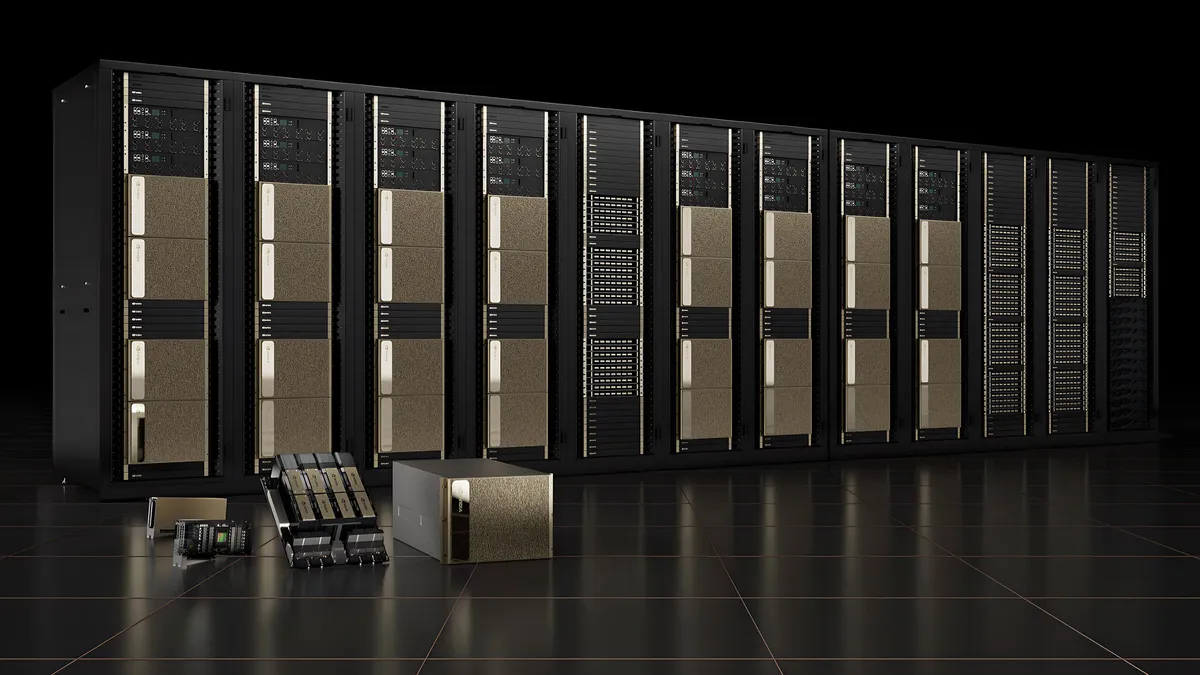
The Nvidia H100 GPU is only part of the story, of course. As with A100, Hopper will initially be available as a new DGX H100 rack mounted server. Each DGX H100 system contains eight H100 GPUs, delivering up to 32 PFLOPS of AI compute and 0.5 PFLOPS of FP64, with 640GB of HBM3 memory. The DGX H100 alos has 3.6 TB/s of bisection bandwidth.

Using multiple DGX H100 servers, Nvidia scales out to a DGX SuperPod with 32 DGX H100 systems, linked together with an updated NVLink Switch system and Quantum-2 InfiniBand networking. A single H100 SuperPod thus has 256 H100 GPUs, 20TB of HBM3 memory, and up to 1 ExaFLOPS of AI compute potential. It also delivers 70.4 TB/s of bisection bandwidth.

Naturally, supercomputers can be built using multiple SuperPods, and Nvidia announced its new Eos supercomputer that follows in the footsteps of Selene. Eos will be built from 18 H100 SuperPods, with 576 DGX H100 systems and 360 NVLink Switches, and it will deliver 275 PFLOPS of FP64 compute. More importantly in Nvidia's AI-focused future, it will deliver 18 EFLOPS of FP8 AI compute, or 9 EFLOPS of FP16.

Hopper, Meet Grace

Nvidia Hopper H100 with Grace CPU "Superchip"

(Image credit: Nvidia)

While so far we've been talking about the Hopper GPU and its various incarnations, there's still the other half of the namesake to discuss, the Grace CPU. We have a separate piece going deeper into what the Nvidia Grace CPU entails, but Nvidia will offer "Grace Hopper Superchips" that combine a Grace CPU with a Hopper GPU on a single module, with a 900 GB/s coherent interface between the two. While Hopper will arrive later this year in the third quarter, the Grace Hopper Superchip won't be available until Q3 2023. Whether those will be used in future DGX servers isn't clear, but Nvidia's CPU aspirations most definitely didn't die with the failure of its Arm acquisition.

Wrapping things up, while it's exciting to hear what Hopper will deliver later this year, we're more interested in what all of this means for the consumer side of things. The previous generation A100 used TSMC 7N (custom N7 for Nvidia), as opposed to Samsung 8N that was utilized for the rest of Nvidia's Ampere lineup. The rumored Ada GPUs will likely also use a slightly less advanced process node than Hopper, but so far all indications are that it will be TSMC N5, which may not be all that different from 4N.

Nvidia likely won't use HBM3 for Ada GPUs, but the fact that Nvidia is promising potentially triple the performance of A100 with Hopper H100 means there's plenty of room left for higher performance consumer parts. Many hope we'll see at least a doubling of performance at the top of the product stack, meaning a hypothetical GeForce RTX 4090 could be twice as fast as the RTX 3090. Given what we've now learned about Hopper, such gains may not be all that farfetched. On the other hand, there are also rumors we could see 600W GeForce GPUs with the next generation, and again Hopper proves Nvidia is willing to push the power envelope in pursuit of performance.

As for Hopper, there's still plenty that we don't know. Presumably the Nvidia H100 coming out later this year won't use a fully enabled GH100 die, as that would result in very low yields, but we don't know how many cores or other elements are present. It looks like Nvidia will stick with six HBM stacks, one of which is for ECC, with 16GB per HBM3 package. Clock speeds are also unknown, and pricing will likely be very high, just like with the previous DGX A100. Nvidia almost certainly has a future DGX H100 based off of its Grace CPU also in the works. As in the past, Nvidia will present a whitepaper on the full Hopper architecture in the near future, and we'll have more to report at that time.

For those interested in the full slide deck, you can see that below. There was a ton of other cool and interesting stuff discussed in the keynote, and if you have the time to watch it (and missed it the first time around), check it out.

Jarred Walton

Jarred Walton is a senior editor at Tom's Hardware focusing on everything GPU. He has been working as a tech journalist since 2004, writing for AnandTech, Maximum PC, and PC Gamer. From the first S3 Virge '3D decelerators' to today's GPUs, Jarred keeps up with all the latest graphics trends and is the one to ask about game performance.

  • peachpuff
    Do the datacenter guys have the same issues with Nvidia gpu stock as the regular folk?
    Reply
  • hotaru.hino
    peachpuff said:
    Do the datacenter guys have the same issues with Nvidia gpu stock as the regular folk?
    No, because they order directly from NVIDIA, who makes the final product. AIBs don't get to touch the "big" GPU products.
    Reply
  • renz496
    peachpuff said:
    Do the datacenter guys have the same issues with Nvidia gpu stock as the regular folk?

    don't think so. some of the professional client already orders 10 of thousands of them in advance. sometimes even before nvidia make their official product announcement. i heard one stories about how one company end up pre-ordering 15k of nvidia GK110 in mid 2012 when the first batch of GK110 chip not coming out until Q4 2012.
    Reply
  • JarredWaltonGPU
    hotaru.hino said:
    No, because they order directly from NVIDIA, who makes the final product. AIBs don't get to touch the "big" GPU products.
    Not to mention, these are in a completely different category of cost. Not even miners are willing to pay the prices that these GPUs command, and scalpers don't factory into the picture either. Buying a $700 GPU and reselling it for $1500 is one thing; buying a $400,000 DGX system and trying to flip it on eBay for even $500,000 isn't going to happen. :-D
    Reply
  • hotaru.hino
    JarredWaltonGPU said:
    Not to mention, these are in a completely different category of cost. Not even miners are willing to pay the prices that these GPUs command, and scalpers don't factory into the picture either. Buying a $700 GPU and reselling it for $1500 is one thing; buying a $400,000 DGX system and trying to flip it on eBay for even $500,000 isn't going to happen. :-D
    I'm pretty sure the government also wants to know why you want to move more than 5 figures worth of money.
    Reply
  • drivinfast247
    hotaru.hino said:
    I'm pretty sure the government also wants to know why you want to move more than 5 figures worth of money.
    They want to know if you move $600 bucks!
    Reply
  • jp7189
    This article makes Hopper sound monolithic with talk of fully enabled die having low yields, etc. Has that been confirmed? I was expecting a shift to MCM on the datacenter lineup this round.
    Reply
  • spongiemaster
    peachpuff said:
    Do the datacenter guys have the same issues with Nvidia gpu stock as the regular folk?
    A regular ol' PCIe A100 costs about $20k ($15k off! It's like Black Friday in March!). Miners aren't touching these, and they are built by TSMC so Nvidia isn't deciding how to allocate their wafers, everything is going to these enterprise GPU's.

    https://www.dell.com/en-us/shop/nvidia-ampere-a100-pcie-300w-80gb-passive-double-wide-full-height-gpu-customer-install/apd/490-bhbk/graphic-video-cards
    Reply
  • spongiemaster
    jp7189 said:
    This article makes Hopper sound monolithic with talk of fully enabled die having low yields, etc. Has that been confirmed? I was expecting a shift to MCM on the datacenter lineup this round.
    Yes. The rumors pointed to MCM, but that appears to be for their upcoming CPU. GH100 is monolithic.
    Reply
  • JarredWaltonGPU
    spongiemaster said:
    Yes. The rumors pointed to MCM, but that appears to be for their upcoming CPU. GH100 is monolithic.
    It's almost like people make up rumors when news is slow! Not mentioning any names... :sneaky::cautious:😠😞
    Reply