Nvidia Unveils 144-core Grace CPU Superchip, Claims Arm Chip 1.5X Faster Than AMD's EPYC Rome
Nvidia enters the CPU business in a big way
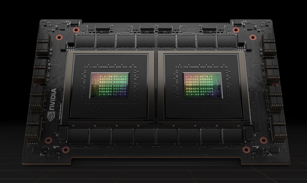
At GTC 2022, Nvidia CEO Jensen Huang finally shared more details around the company's Arm endeavors as he unveiled the company's new 144-core Grace CPU Superchip, the company's first CPU-only Arm chip designed for the data center. The Neoverse-based system supports Arm v9 and comes as two CPUs fused together with Nvidia's newly branded NVLink-C2C interconnect tech. Nvidia claims the Grace CPU Superchip offers 1.5X more performance in a SPEC benchmark than two of the last-gen 64-core AMD EPYC processors in its own DGX A100 servers, and twice the power efficiency of today's leading server chips. Overall, Nvidia claims the Grace CPU Superchip will be the fastest processor on the market when it ships in early 2023 for a wide range of applications, like hyperscale computing, data analytics, and scientific computing.
Given what we know about Arm's roadmap, the Hopper CPU Superchip is based on the N2 Perseus platform, the first to support Arm v9. This platform comes as a 5nm design that supports all of the latest connectivity tech, like PCIe Gen 5.0, DDR5, HBM3, CCIX 2.0 and CXL 2.0, delivering up to 40% more performance over the V1 platform.
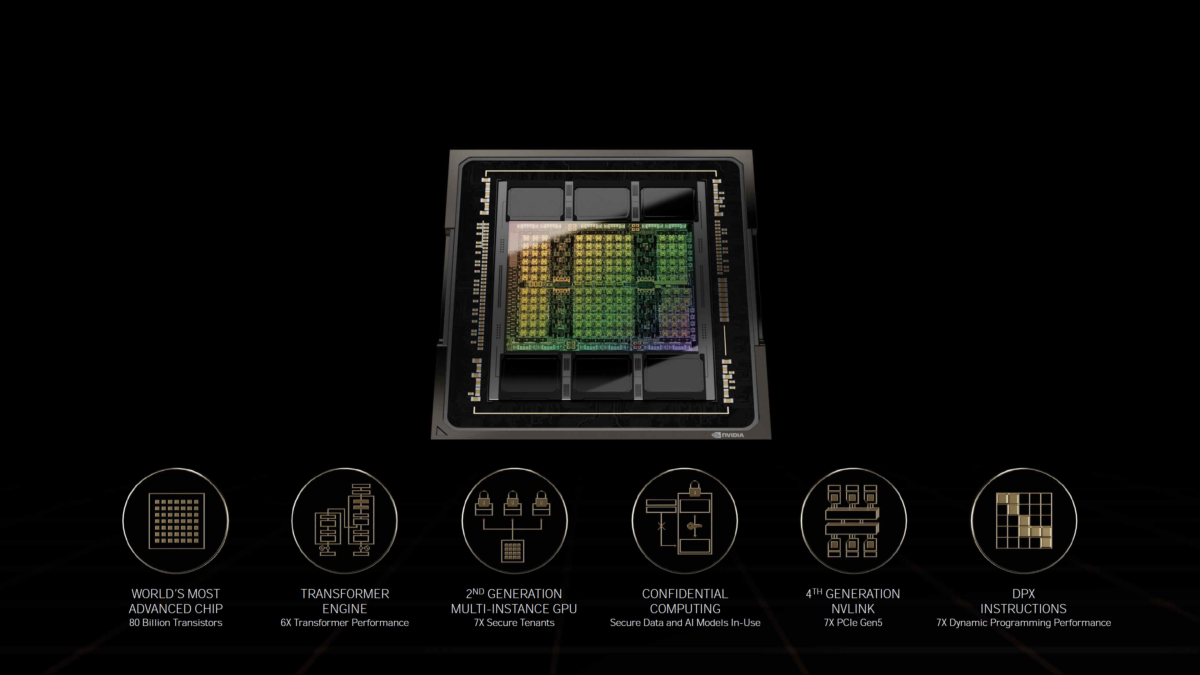
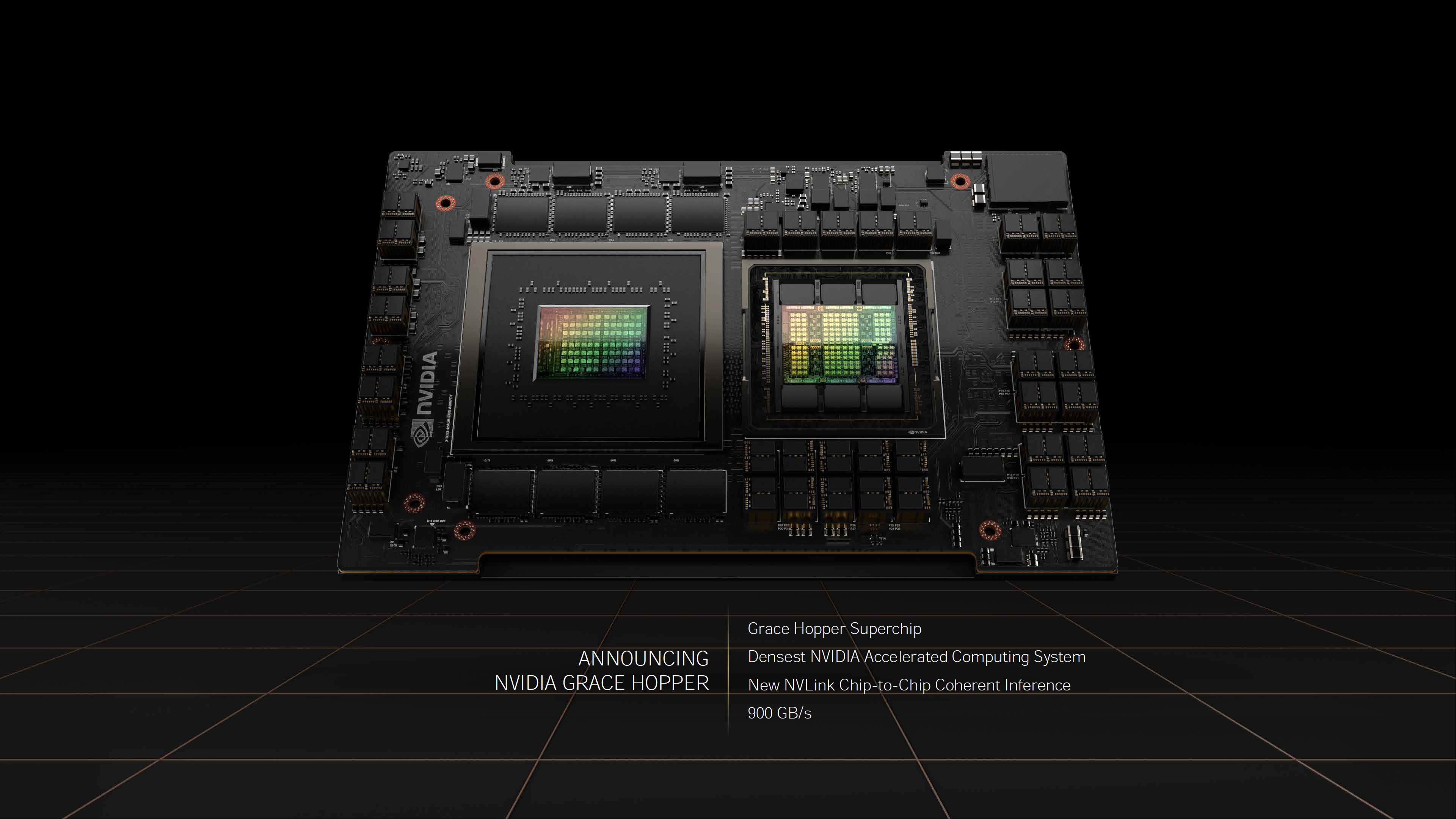
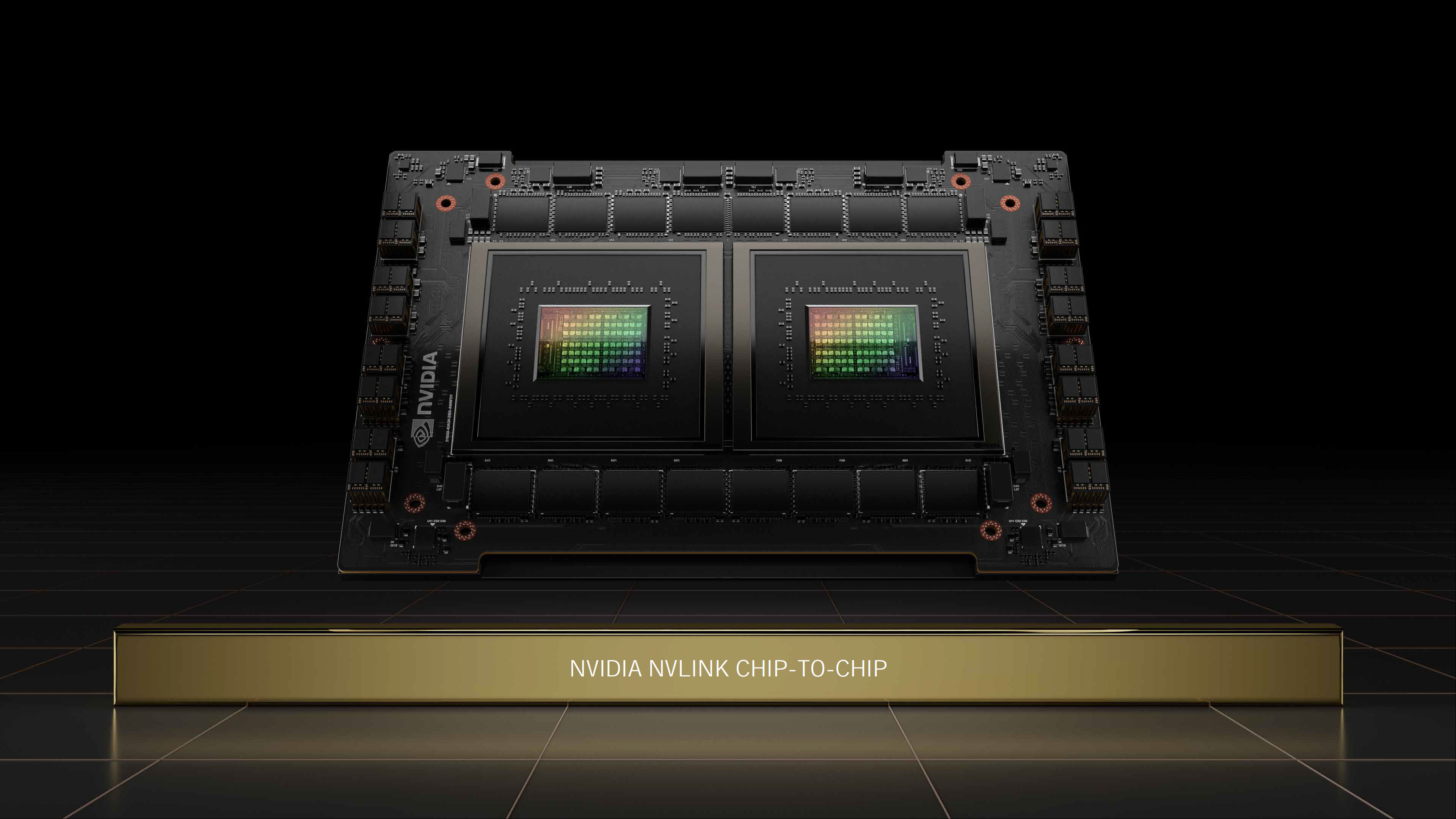
Additionally, Nvidia shared new details about the Grace Hopper Superchip, its previously-announced CPU+GPU chip. Nvidia also announced its new NVLink Chip-to-Chip (C2C) interface, a die-to-die and chip-to-chip interconnect that supports memory coherency. NVLink-C2C can provide up to 25x more energy efficiency and is 90x more area-efficient than the PCIe 5.0 PHYs Nvidia currently uses, supporting up to 900 GB/s of throughput or higher. This interface supports industry-standard protocols like CXL and Arm's AMBA CHI and supports connections ranging from PCB-based interconnects to silicon interposers and wafer-scale implementations. Surprisingly, Nvidia is now allowing other vendors to use the design for their own chiplets. Additionally, Nvidia announced that it would support the new UCIe specification. Let's dive in on the details.
Nvidia Grace CPU Superchip
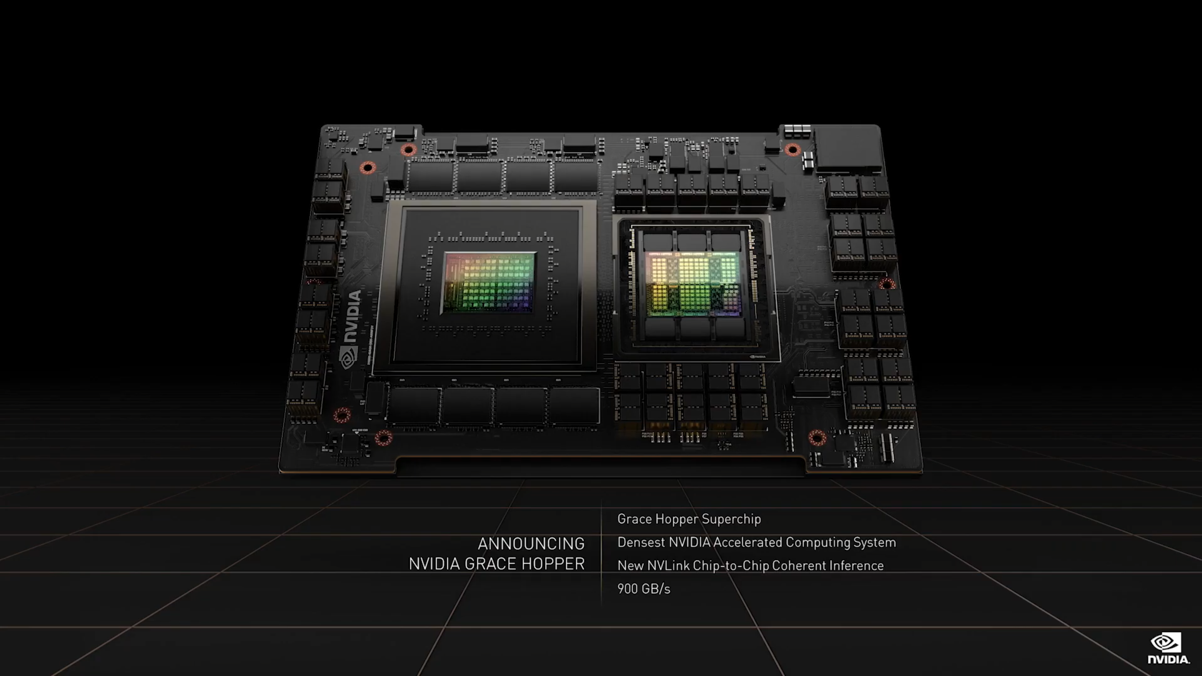
Before we get to the new Grace CPU Superchip, you'll need a quick refresher on its first instantiation. Nvidia first announced what it originally called its Grace CPU last year, but the company didn't share too many fine-grained details. Nvidia has now changed the name of this first effort to the Grace Hopper Superchip.
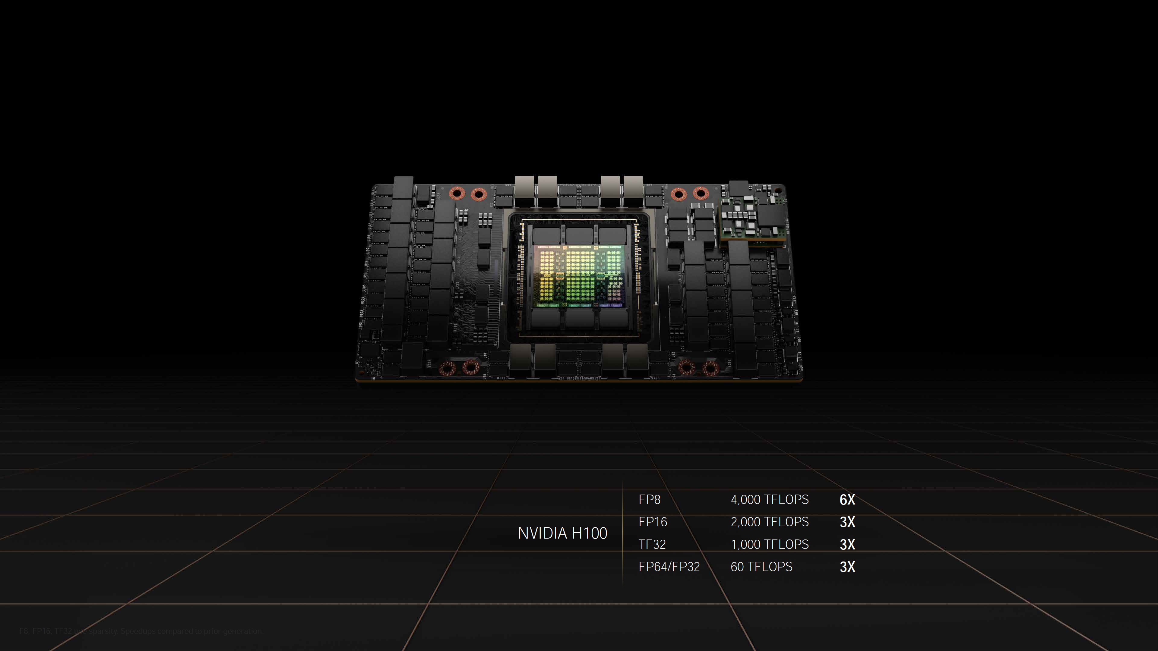
The Grace Hopper Superchip has two distinct chips, one CPU and one GPU, on one carrier board. We now know the CPU has 72 cores, uses a Neoverse-based design that supports Arm v9, and it's paired with a Hopper GPU. These two units communicate over a 900 GBps NVLink-C2C connection that provides memory coherency between the CPU and GPU, thus allowing both units to have simultaneous access to the pool of LPDDR5X ECC memory that has a claimed 30X bandwidth improvement over standard systems.
Nvidia originally didn't announce the amount of LPDDR5X used for the design, but here we can see that the company now claims a '600GB Memory GPU,' which assuredly includes the LPDDR5X memory pool. We know that LPDDR5X tops out at 64GB per package, meaning the CPU comes with up to 512 GB of LPDDR5X. Meanwhile, the Hopper GPU typically has 80GB of HBM3 capacity, placing us near Nvidia's 600GB figure. Giving the GPU access to that amount of memory capacity could have a transformative effect for some workloads, particularly for properly-optimized applications.
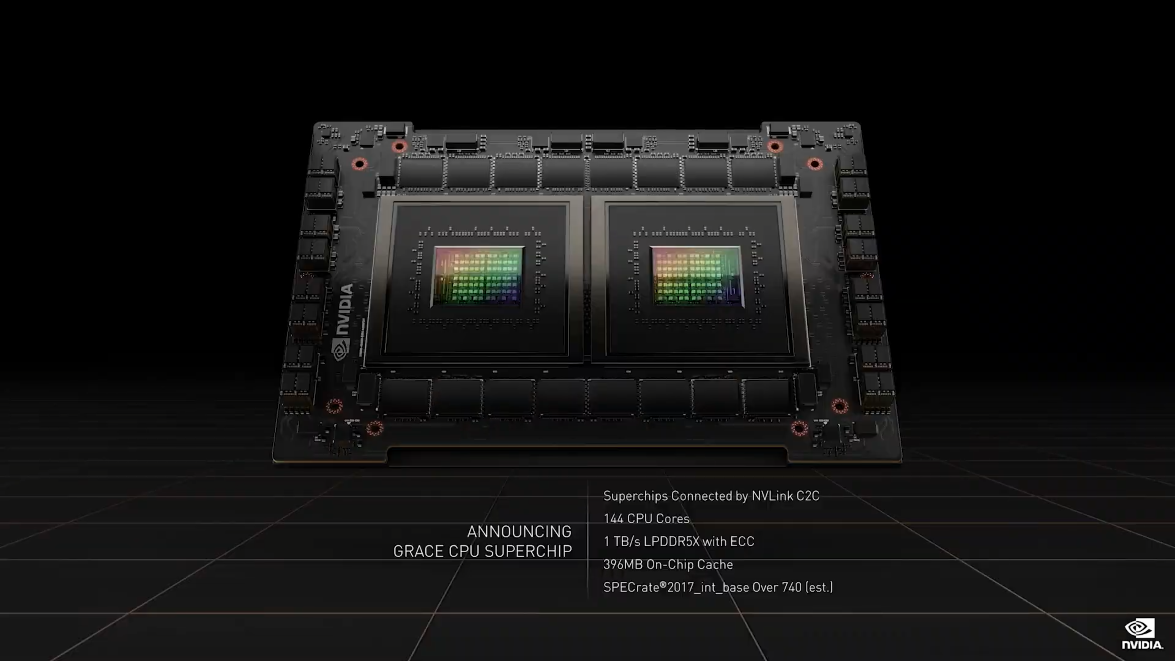
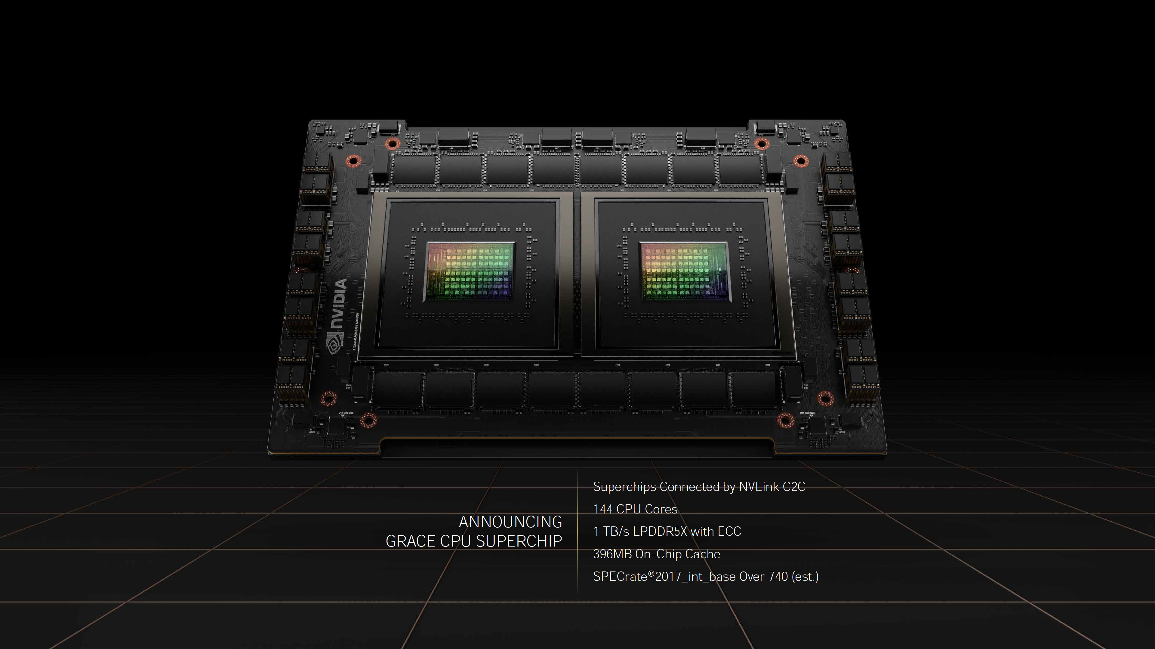
Today's announcement covers the Grace CPU Superchip, which is based on the Grace Hopper CPU+GPU design but uses a second CPU package instead of the Hopper GPU. These two 72 core chips are also connected via the NVLink-C2C connection, providing a coherent 900 GB/s connection that melds them into one 144-core unit. In addition, the Arm v9 Neoverse-based chip supports Arm's Scalable Vector Extensions (SVE), which are performance-boosting SIMD instructions that function similar to AVX.
The Grace CPU Superchip uses Arm v9, which tells us that the chip uses the Neoverse N2 design that you can read about in more depth here. The Neoverse N2 platform is Arm's first IP to support newly-announced Arm v9 extensions like SVE2 and Memory Tagging and delivers up to 40% more performance over the V1 platform. The N2 Perseus platform comes as a 5nm design supporting PCIe Gen 5.0, DDR5, HBM3, CCIX 2.0, and CXL 2.0. The Perseus design is optimized for performance-per-power (watt) and performance-per-area.
That makes plenty of sense given that the Grace CPU Superchip consumes a peak of 500W for both the two CPUs and the onboard memory. That is competitive with other leading CPUs, like AMD's EPYC, which tops out at 280W per chip (this doesn't include memory power consumption). Nvidia claims the Grace CPU will be twice as efficient as competing CPUs when it comes to market.
Each CPU has access to its own eight LPDDR5X packages, so the two chips will still be influenced by the standard NUMA-like tendencies of near and far memory. Still, the increased bandwidth between the two chips should also help reduce latency due to less contention, thus making for a very efficient multi-chip implementation. The device also comes with 396MB of on-chip cache, but it isn't clear if that is for a single chip or both.
The Grace CPU Superchip memory subsystem provides up to 1TB/s of bandwidth, which Nvidia says is a first for CPUs and more than twice that of other data center processors that will support DDR5 memory. The LPDDR5X comes spread out in 16 packages that provide 1TB of capacity. In addition, Nvidia notes that Grace uses the first ECC implementation of LPDDR5X.
This brings us to benchmarks. Nvidia claims the Grace CPU Superchip is 1.5X faster in the SPECrate_2017_int_base benchmark than the two previous-gen 64-core EPYC Rome 7742 processors it uses in its DGX A100 systems. Nvidia based this claim on a pre-silicon simulation that predicts the Grace CPU at a score of 740+ (370 per chip). AMD's current-gen EPYC Milan chips, the current performance leader in the data center, have posted SPEC results ranging from 382 to 424 apiece, meaning the highest-end x86 chips will still hold the lead. However, Nvidia's solution will have many other advantages, such as power efficiency and a more GPU-friendly design.
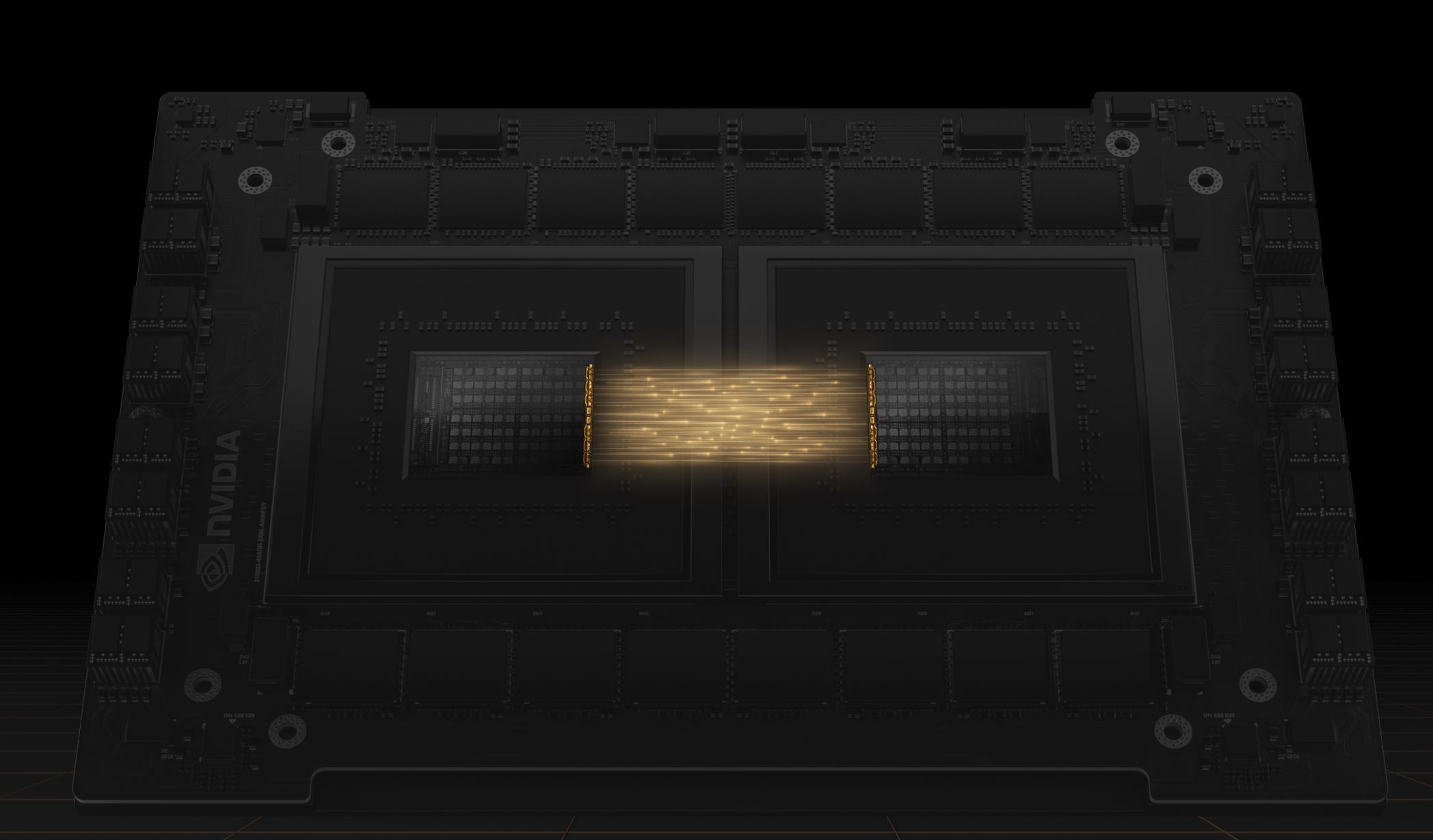
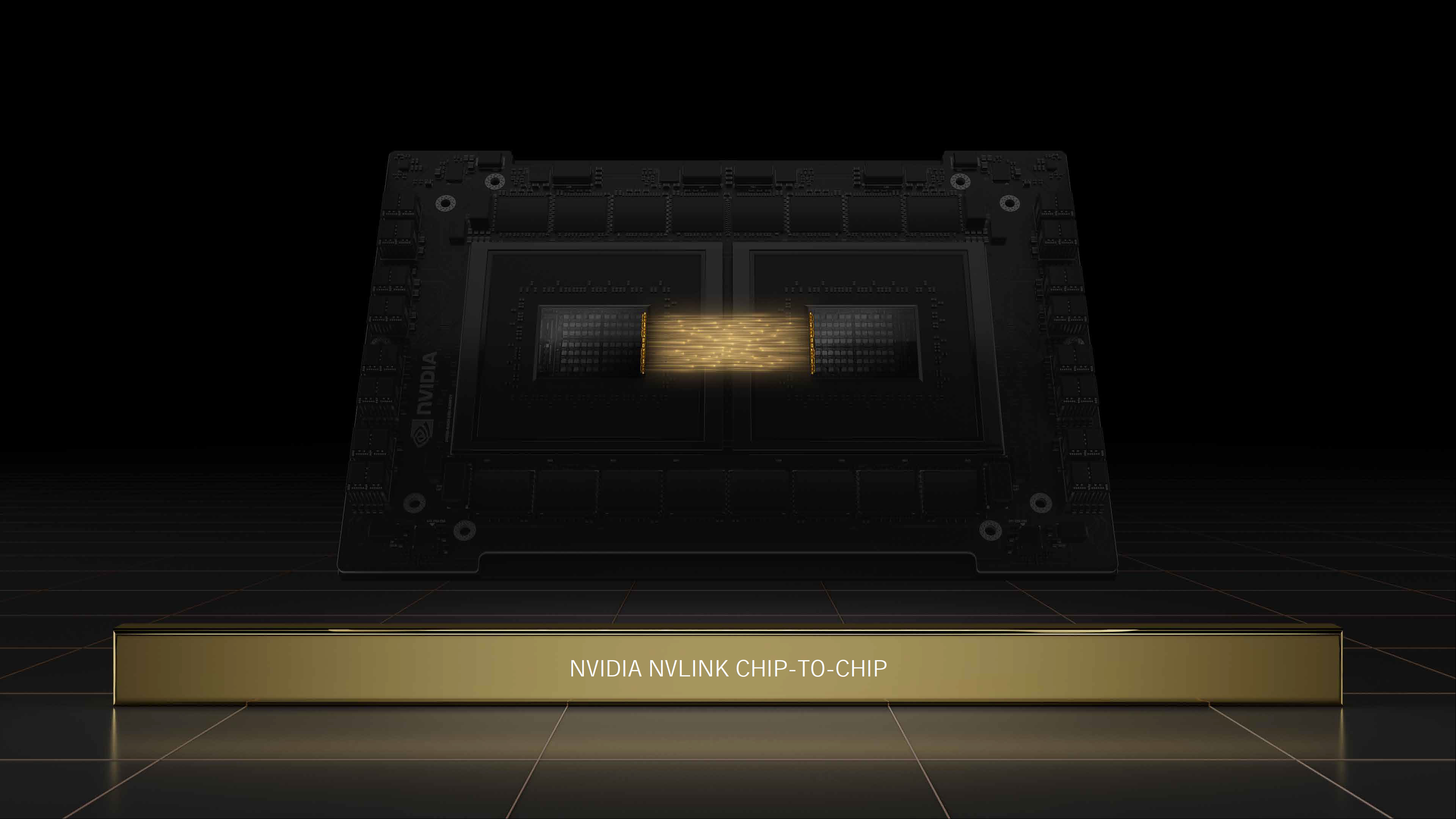
The two Grace CPUs communicate over Nvidia's new NVLink Chip-to-Chip (C2C) interface. This die-to-die and chip-to-chip interconnect supports low-latency memory coherency, allowing the connected devices to work on the same pool of memory simultaneously. Nvidia crafted the interface using its SERDES and LINK design technologies with a focus on energy and area efficiency.
Nvidia says NVLink-C2C can provide up to 25x more energy efficiency and is 90x more area-efficient than the PCIe 5.0 PHYs Nvidia currently uses, supporting up to 900 GB/s of throughput or higher. In addition, this interface supports industry-standard protocols like CXL and Arm's AMBA Coherent Hub Interface (CHI). It also supports several types of connections ranging from PCB-based interconnects to silicon interposers and wafer-scale implementations.
Support for AMBA CHI is important, and Neoverse supports Arm's Coherent Mesh Network (CMN-700) that will tie together the N2 designs with intelligent high-bandwidth low-latency interfaces to other platform additives, such as DDR, HBM, and various accelerator technologies, using a combination of industry-standard protocols, like CCIX, CXL, and PCIe. This new mesh design serves as the backbone for the next generation of Arm processors based on both single-die and multi-chip designs. You can read more about the protocol here.
Nvidia also announced that it would support the new UCIe chiplet interconnect standard supported by other industry heavyweights, like Intel, AMD, Arm, TSMC, and Samsung. This standardized die-to-die interconnect is designed to provide communication between chiplets with an open-source design, thus reducing costs and fostering a broader ecosystem of validated chiplets. In the end, the UCIe standard aims to be just as ubiquitous and universal as other connectivity standards, like USB, PCIe, and NVMe, while providing exceptional power and performance metrics for chiplet connections. Nvidia's support for this new initiative means that we could theoretically see Nvidia CPU chiplets placed in the same package with competing chip designs in the future.
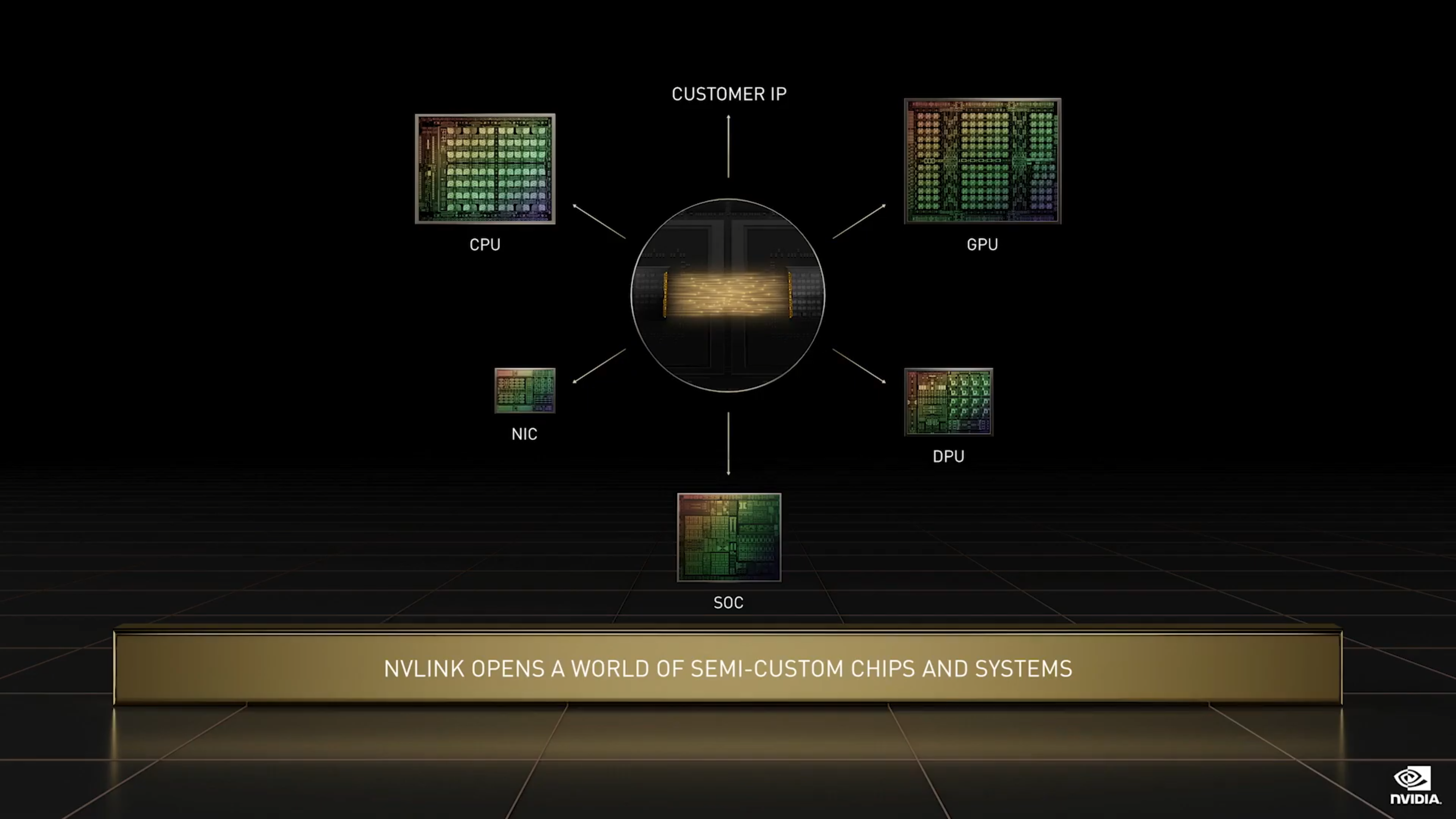
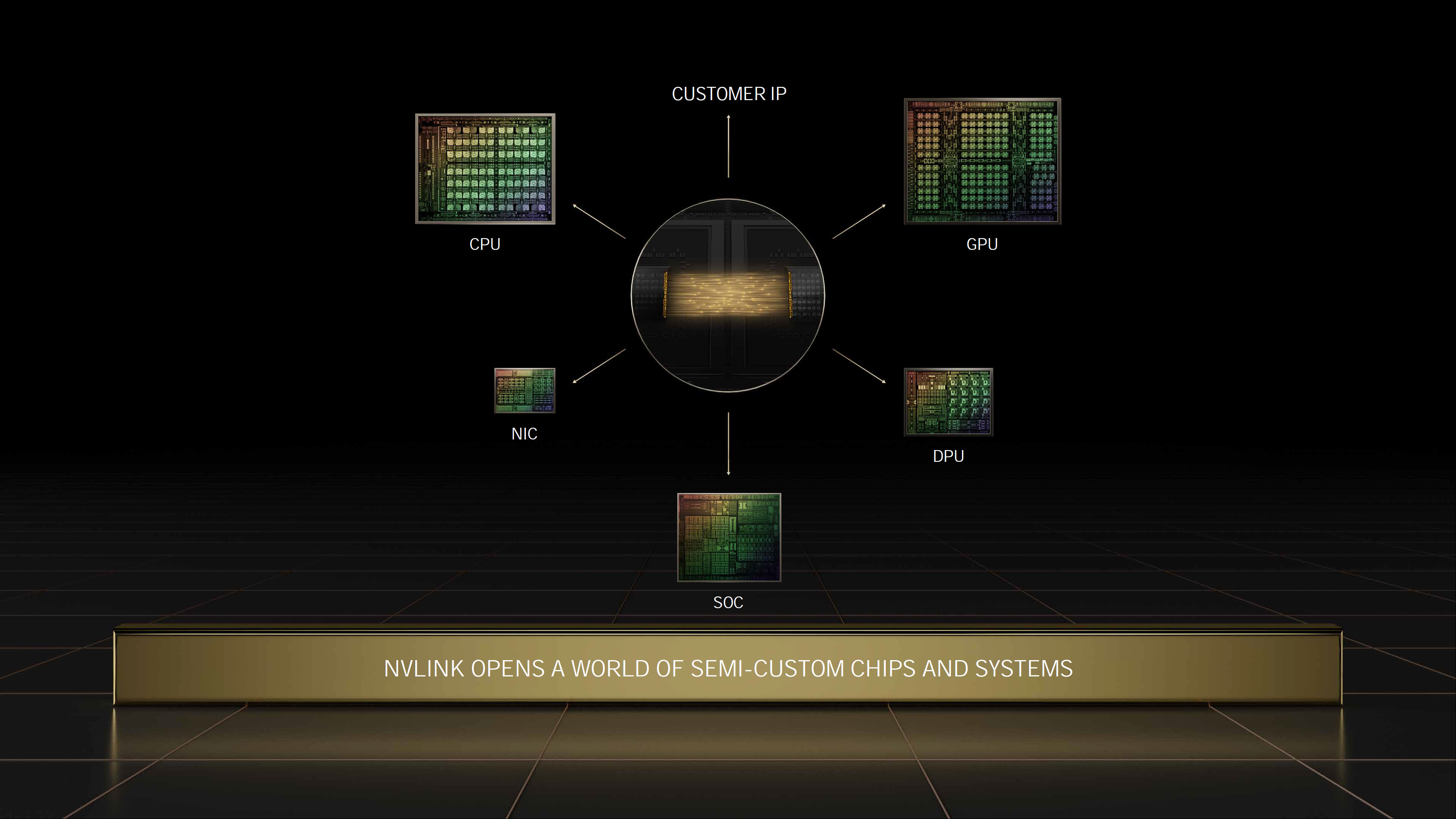
NVLink-C2C will now span to all of Nvidia's silicon, including GPUs, CPUs, SOCs, NICs, and DPUs. Nvidia also says it is opening up the specification to allow other companies to use NVLink in their chiplet designs. That gives customers an option of employing either the UCIe interface or NVLink, though Nvidia claims NVLink-C2C is optimized for lower latency, higher bandwidth, and greater power efficiency than UCIe.
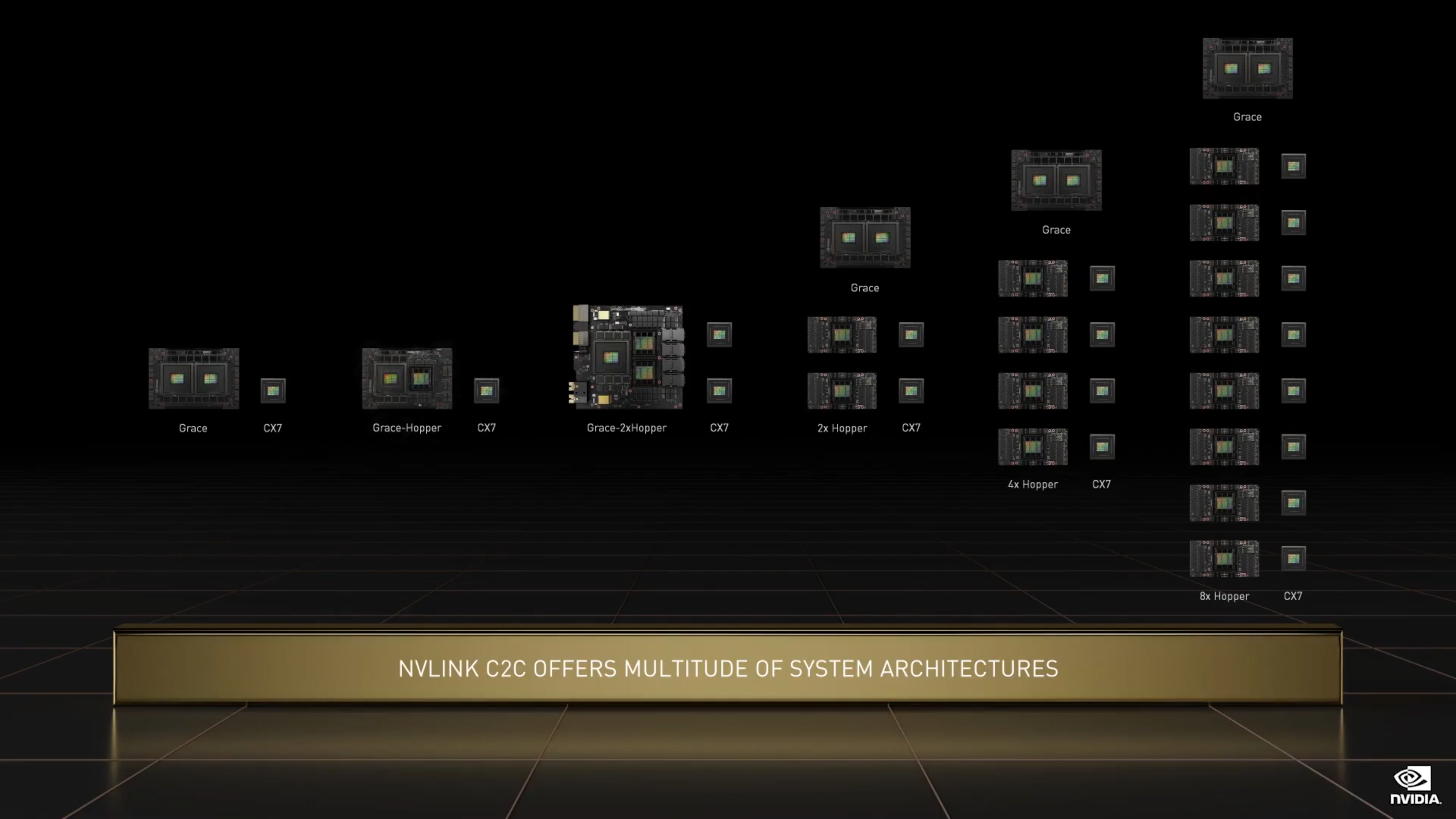
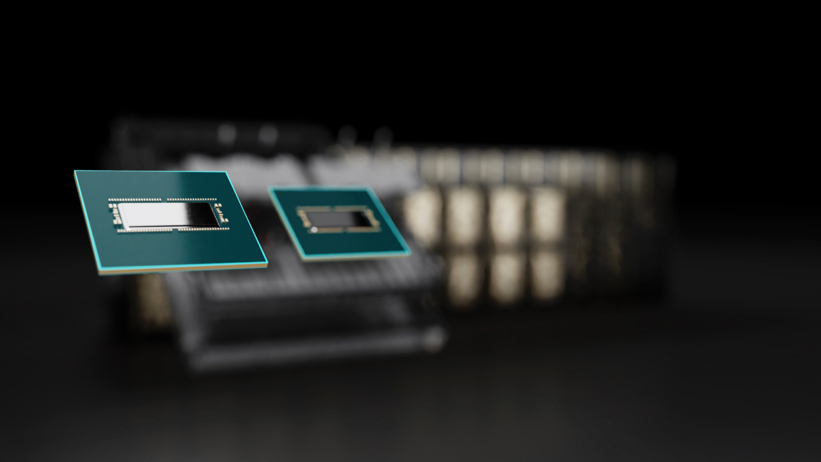
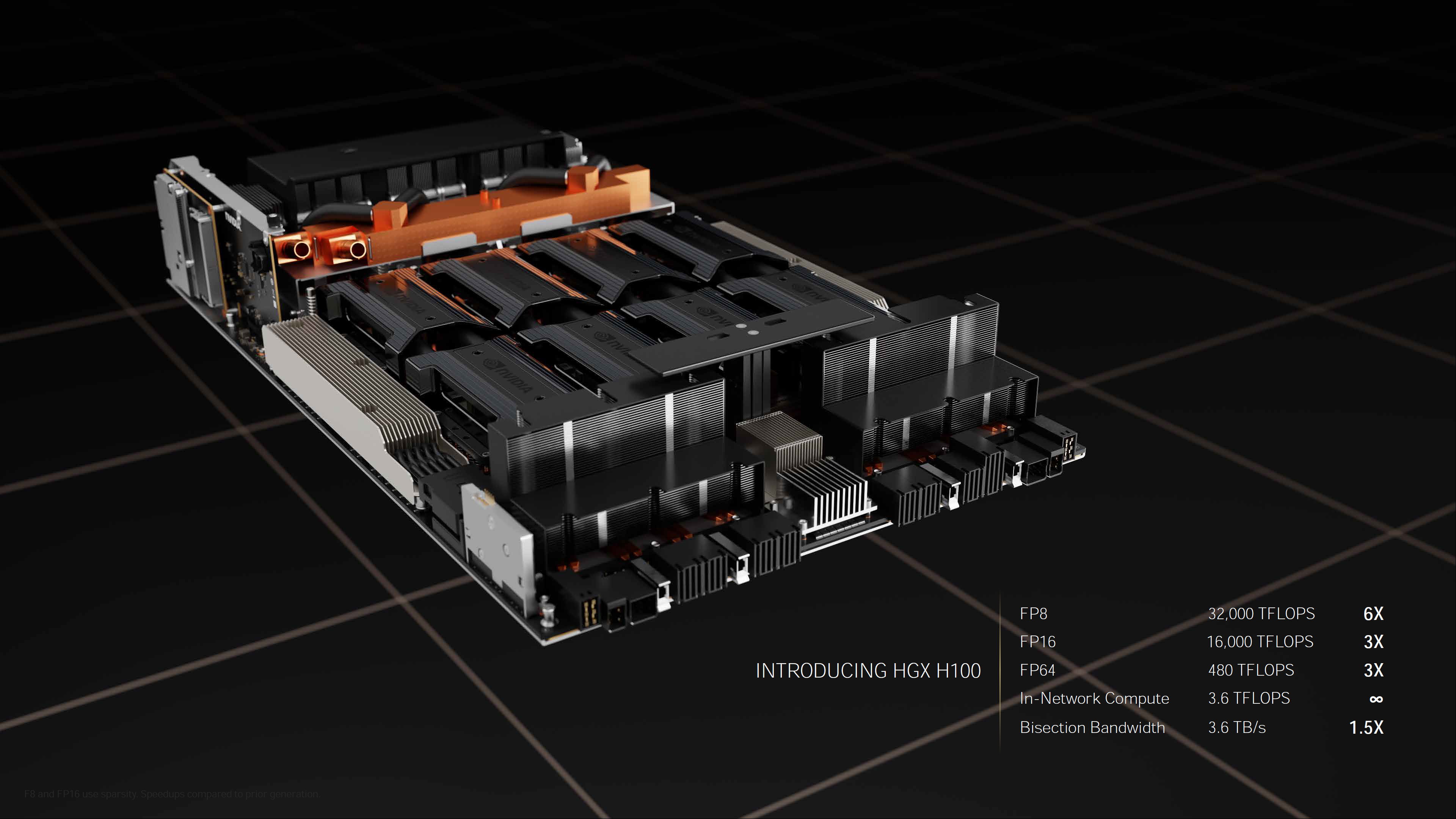
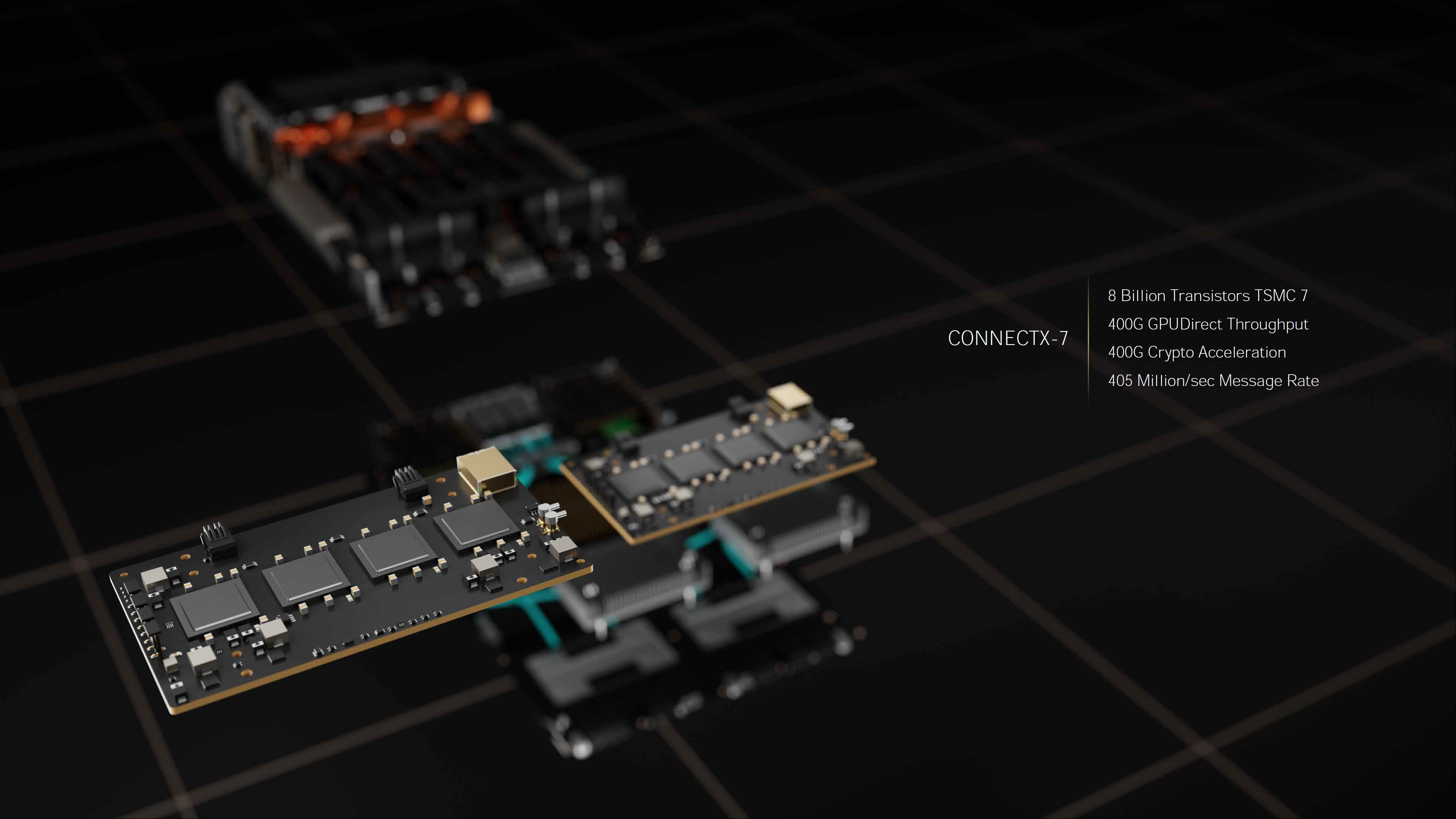
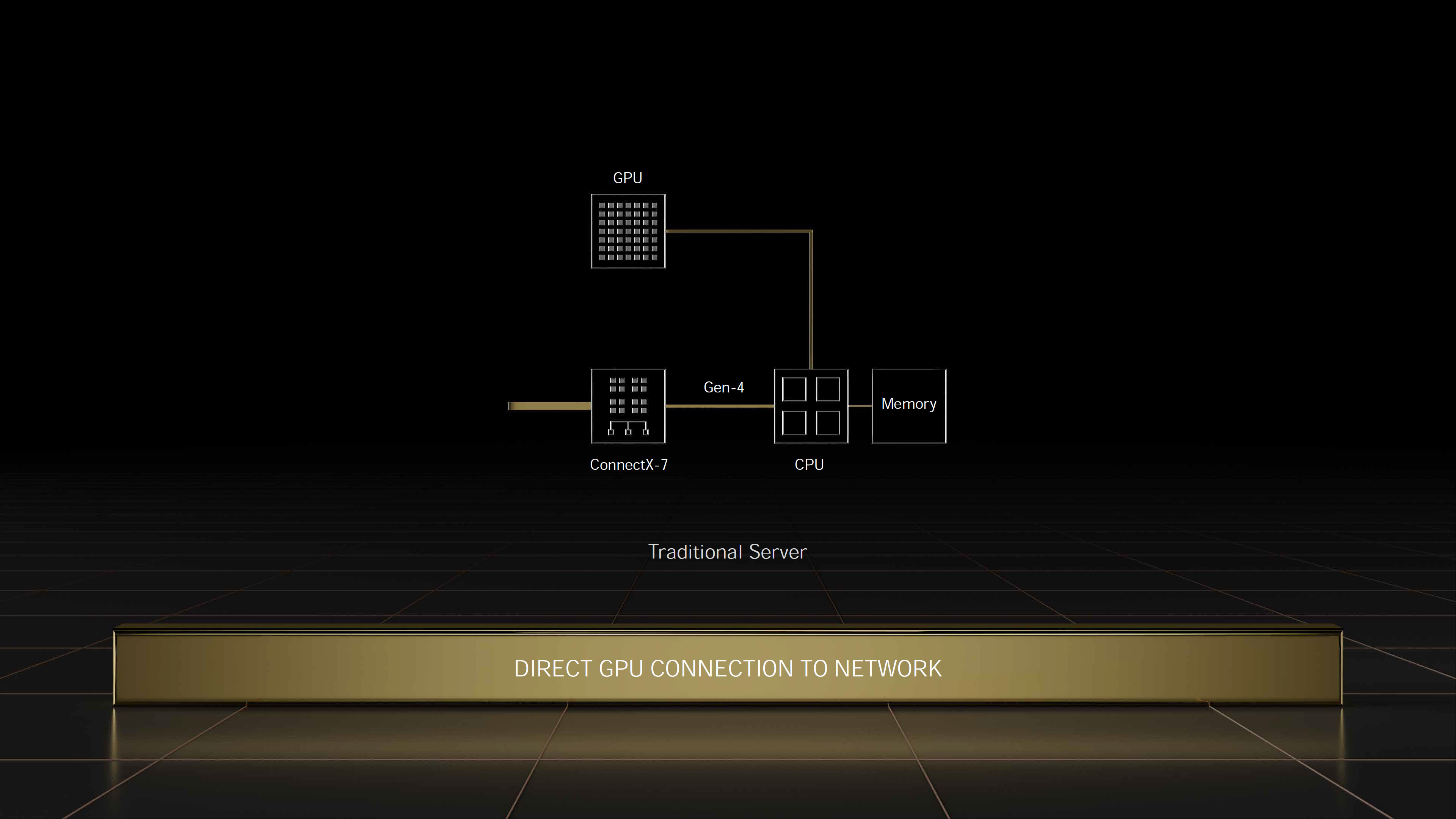
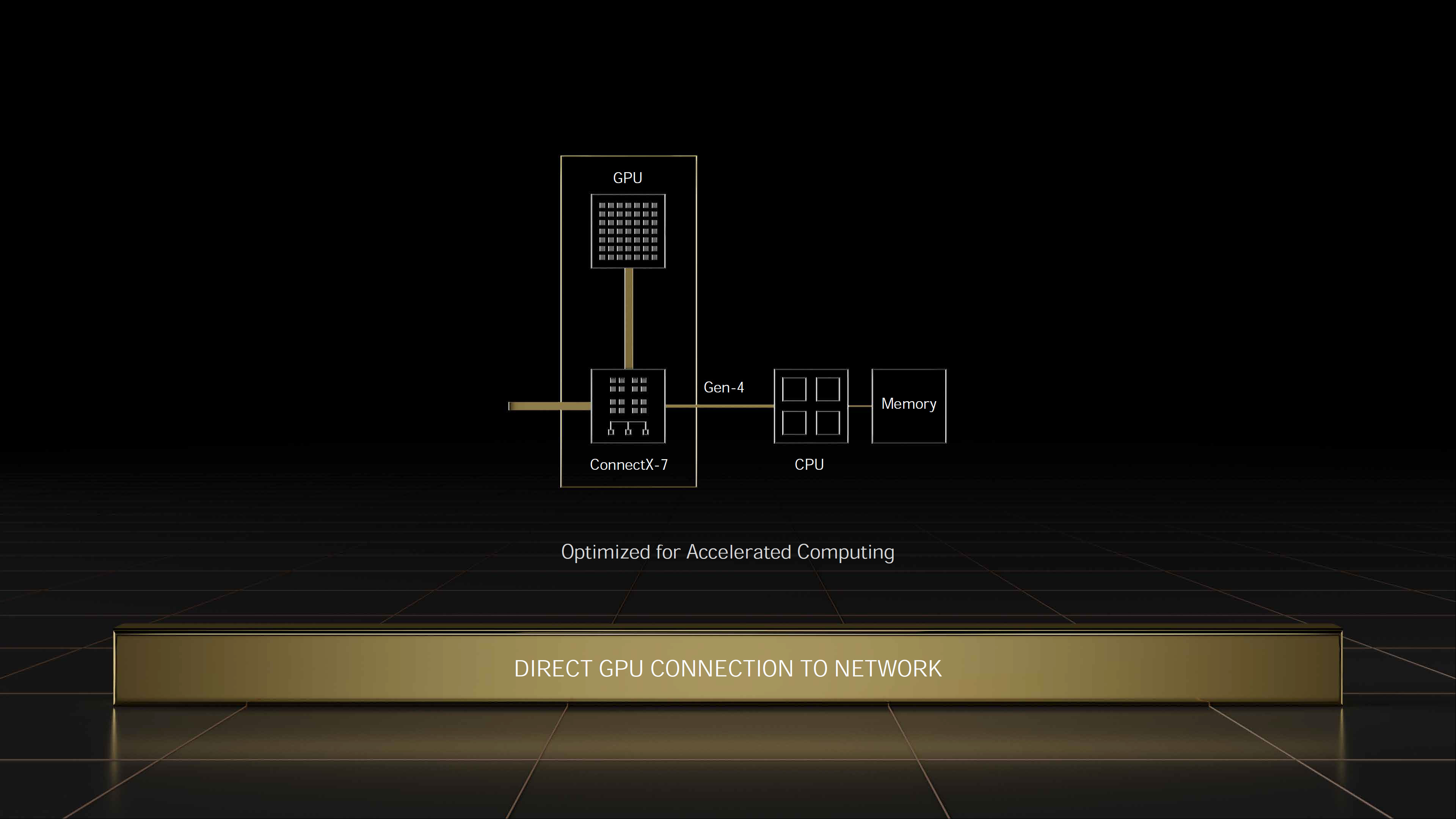
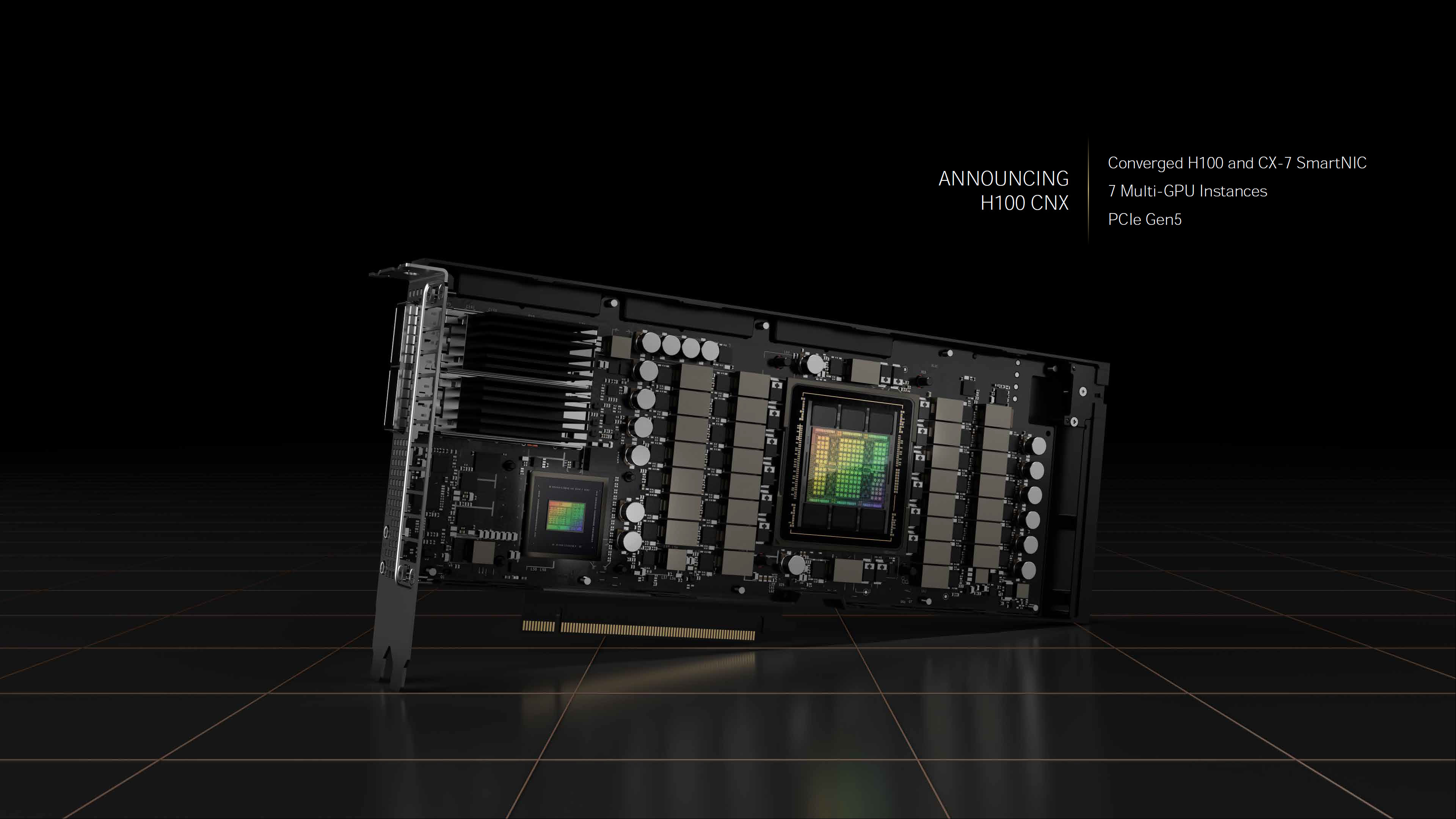
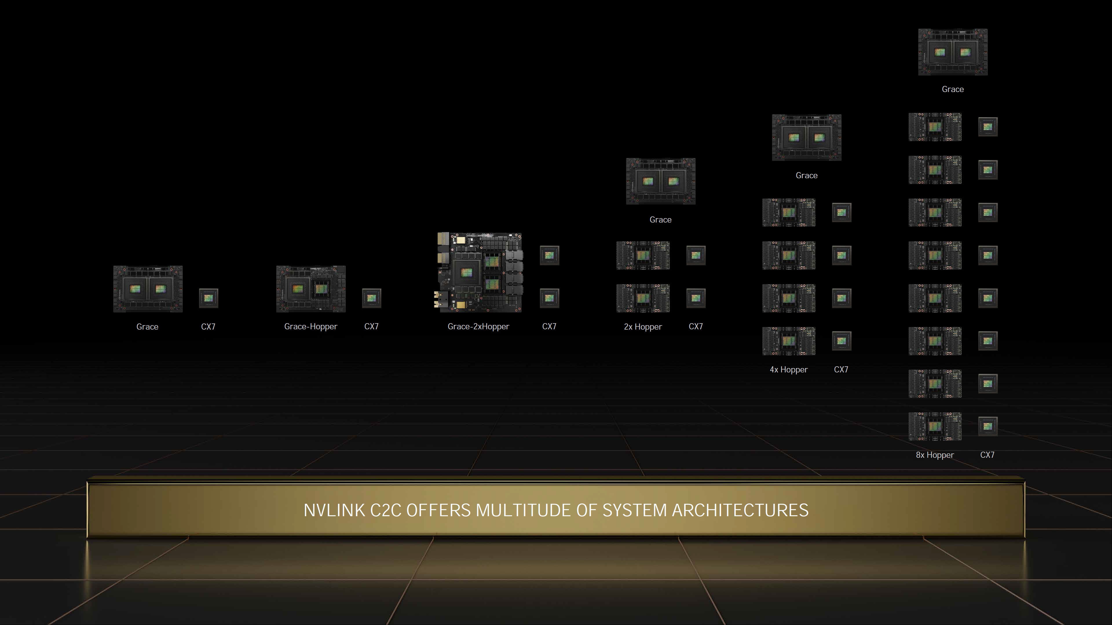
As depicted in the graphic above, the Grace Hopper Superchip and Grace CPU Superchip systems can also be combined in several different configurations with up to eight Hopper GPUs. These designs use Nvidia's ConnectX-7 SmartNICs (CX7) that enable NVLink communication via their in-built PCIe 5.0 switch, thus supporting much more expansive system-to-system applications.
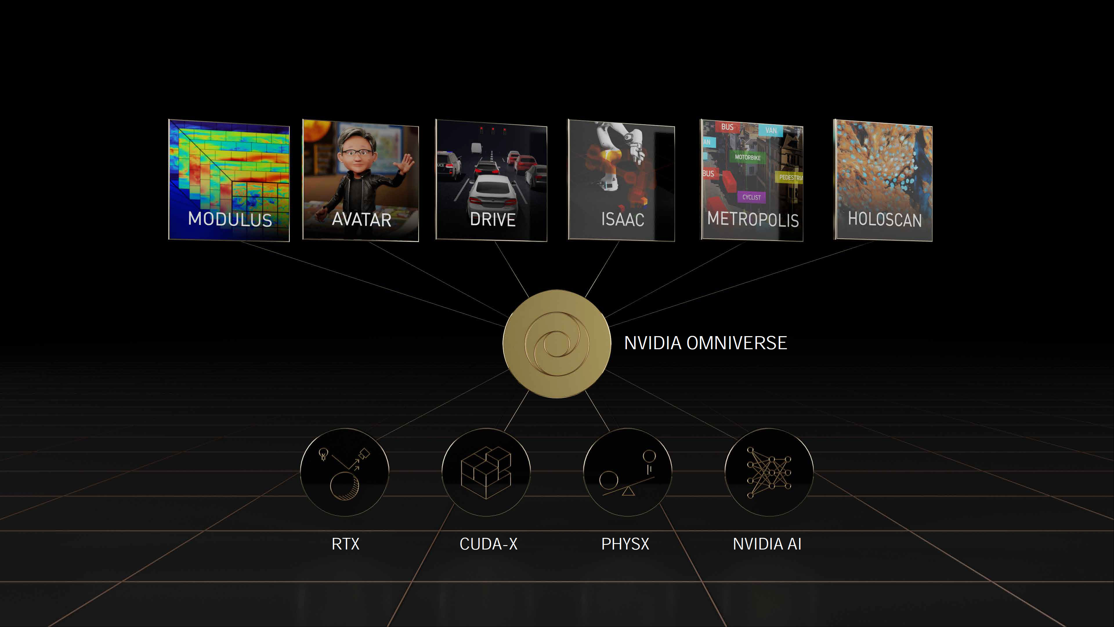
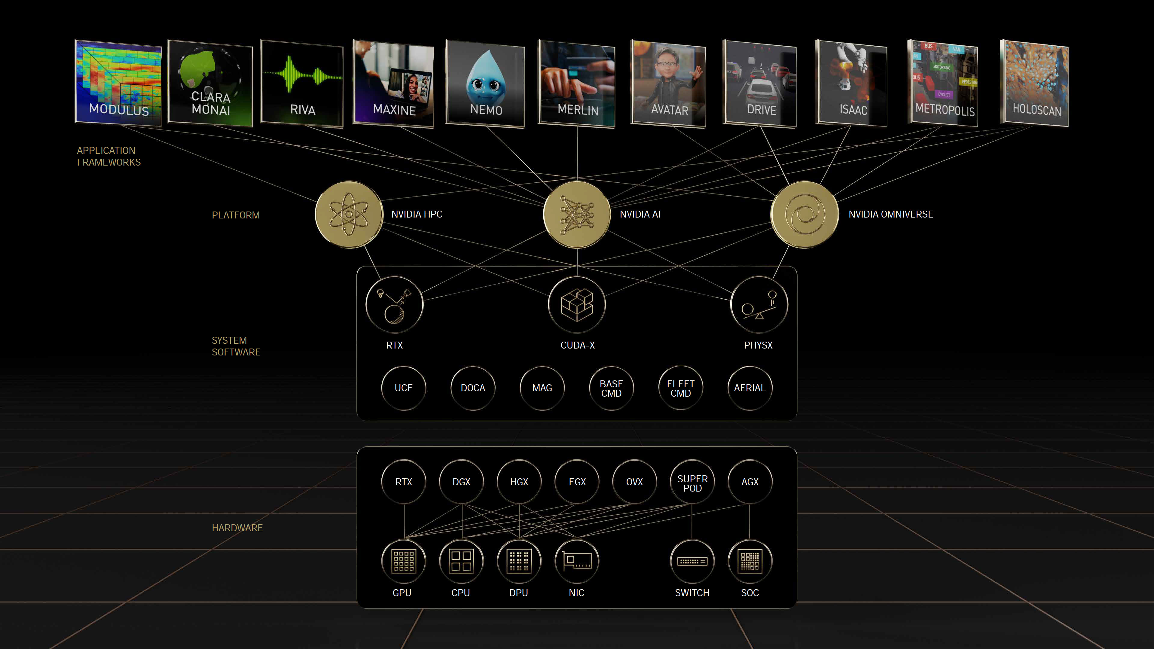
Nvidia is expanding its target markets with the Grace CPU Superchip, now encompassing hyperscale computing, cloud, data analytics, HPC, and AI workloads, effectively targeting the general-purpose server market. The Grace CPU Superchip supports Nvidia's entire CUDA stack and will run the full gamut of Nvidia's applications, including Nvidia RTX, Nvidia AI, HPC, and Omniverse. The chips begin shipping in the first half of 2023.
Nvidia says that it will have a whitepaper coming that provides more granular details about the architecture, which we'll be following closely.
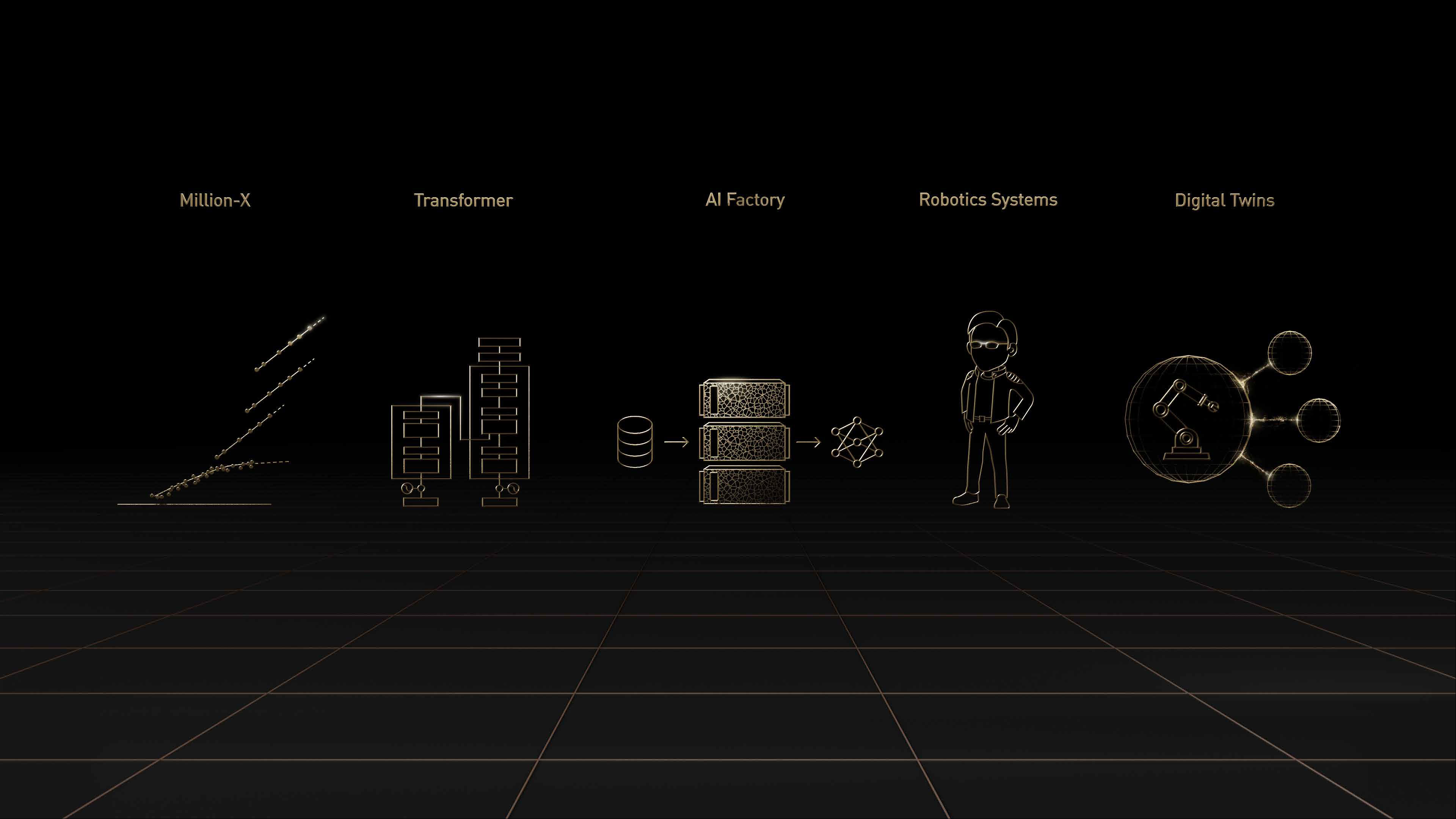
For those interested in the full GTC 2022 keynote slide deck, we've included that below.

































Get Tom's Hardware's best news and in-depth reviews, straight to your inbox.

Paul Alcorn is the Editor-in-Chief for Tom's Hardware US. He also writes news and reviews on CPUs, storage, and enterprise hardware.
-
Liquidrider Looks like Nvidia is more worried about AMD than they are about Intel. Can tell because they didn't compare their chips to Xeon at all. Instead focusing on AMD's 2020 release of Epyc Rome. That doesn't exactly scream homerun, but impressive none the less.Reply
Regardless, I am noticing Intel is becoming more and more an outsider in the server CPU space even by the likes of their own competition. -
jeremyj_83 Reply
Rome was released in August 2019.Liquidrider said:Looks like Nvidia is more worried about AMD than they are about Intel. Can tell because they didn't compare their chips to Xeon at all. Instead focusing on AMD's 2020 release of Epyc Rome. That doesn't exactly scream homerun, but impressive none the less.
Regardless, I am noticing Intel is becoming more and more an outsider in the server CPU space even by the likes of their own competition. -
renz496 ReplyLiquidrider said:Looks like Nvidia is more worried about AMD than they are about Intel. Can tell because they didn't compare their chips to Xeon at all. Instead focusing on AMD's 2020 release of Epyc Rome. That doesn't exactly scream homerun, but impressive none the less.
Regardless, I am noticing Intel is becoming more and more an outsider in the server CPU space even by the likes of their own competition.
because that's what they used on their DGX A100? the future DGX will use nvidia in house Grace ARM CPU. -
Neilbob All it takes is a single benchmark to be faster in order to claim the same performance margin applies to everything.Reply
A wait-and-see approach is always needed when manufacturers start spouting numbers. -
spongiemaster Reply
Exactly. The A100 based DGX system uses dual 7742 Rome based Epyc CPU's. Nvidia is comparing their new CPU's to the one's they are currently using.renz496 said:because that's what they used on their DGX A100? the future DGX will use nvidia in house Grace ARM CPU. -
spongiemaster Reply
These DGX boxes aren't general purpose servers, they are used for pretty specific tasks. If Nvidia designed these CPU's in house, we can be pretty sure they tuned them for use cases relevant to the target market.Neilbob said:All it takes is a single benchmark to be faster in order to claim the same performance margin applies to everything.
A wait-and-see approach is always needed when manufacturers start spouting numbers. -
msroadkill612 Reply
This is the elephant in the room i suspect.spongiemaster said:These DGX boxes aren't general purpose servers, they are used for pretty specific tasks.
Its a spoiler announcement re a 2023 future product, in a series that has lacked the impact of the holistic epyc+GPU platform, & more a reflection of how scary the new gpuS from amd are considering the failed ARM deal.
what NV can do w/ arm, amd can dobetter on Infinity Fabric mixed with Xilinx FGPA magic. -
Makaveli lol what is with both intel and nvidia cherry picking 2 year old AMD hardware to benchmark against the current offerings.Reply
First intel using the old threadrippers and now NV using Rome and not Milan for their benchmarks. -
HideOut compairing to a pretty old chip when AMD's newer faster chips are out. Saying "early 2023" and by then intel and AMD will likely have updated. And its not X86. Fail.Reply
