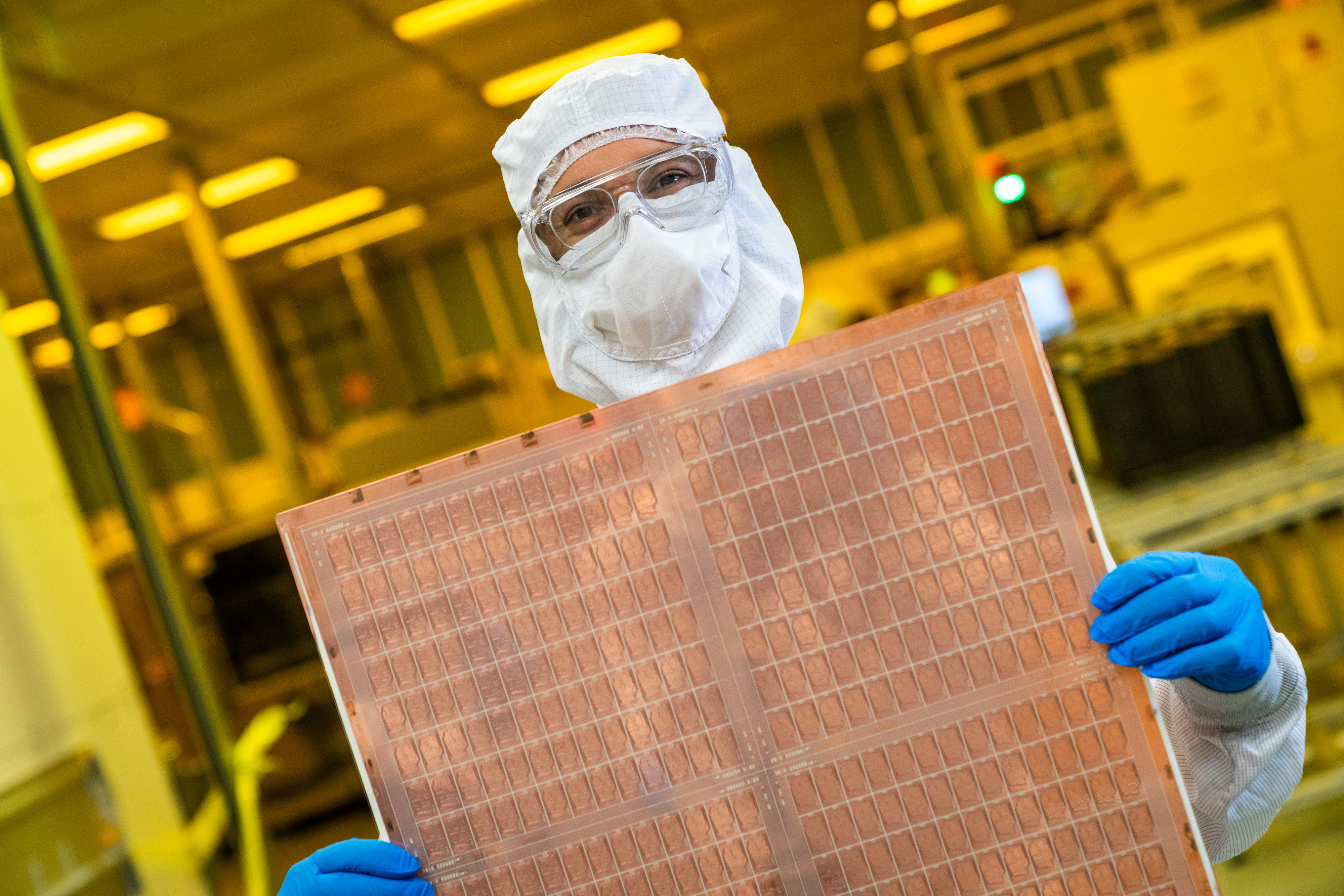
AMD is reportedly set to use glass substrates for CPUs between 2025 and 2026
Glass substrates offer significant benefits over conventional organic substrates.

According to an unconfirmed report from Business Korea, AMD intends to adopt glass substrates for its ultra-high-performance system-in-packages (SiPs) between 2025 and 2026. The report claims the company will work with 'global components companies' on the project. While glass substrates for processors are exotic today, they may be closer to adoption than one might think.
Glass substrates provide notable benefits over conventional organic substrates, so Intel, Samsung, and some other companies are racing to use them in the second half of the decade. The exceptional flatness of glass substrates enables the improved depth of focus for lithography and dimensional stability and is ideal for interconnects in advanced SiPs containing multiple chiplets. Furthermore, glass substrates offer superior thermal and mechanical strength, making them well-suited for high-temperature and durable applications, such as data center-oriented SiPs. That said, glass substrates make great sense for companies like AMD, Intel, and Nvidia.
Two things to consider when reading rumors about AMD's plans to adopt glass substrates in the next couple of years are what AMD will use glass substrates for and why it will do so in the said timeframe.
The answer to the first question is relatively simple: for its data center products aimed at AI and HPC workloads. Performance requirements for AI and, eventually, AGI applications are almost infinite, so processors for artificial general intelligence workloads are poised to adopt the latest technologies to get all the speed they can.
There are two answers to the second one; they are a bit more complicated but relatively obvious. Leading-edge process technologies are getting more expensive (and sometimes more complex to yield), and their transistor density gain is getting smaller. Building large monolithic chips is becoming more costly than creating several smaller chiplets and placing them on an interposer or a substrate from a yield perspective. Furthermore, more performance gains can be obtained by adding chiplets than just using a new production node.
AMD already builds system-in-packages with 13 chiplets (EPYC 9004-series) or even 22 pieces of silicon (Instinct MI300A: 3 Zen 4 CCDs + 6 CDNA 3 compute dies + 4 input/output dies with Infinity Cache + 8 HBM3 stacks + 1 2.5D interposer). Assuming that its future products will get even more complex, it is natural for the company to adopt glass substrates sooner rather than later, given all the advantages they promise to bring.
Another reason to adopt a glass substrate is that it can enable dense interconnects without an interposer, which might lower the pricing of SiPs with many chiplets as interposers tend to be expensive.
Get Tom's Hardware's best news and in-depth reviews, straight to your inbox.
While it makes a lot of sense for AMD to adopt glass substrate packaging in the coming years, we are not sure about the exact 2025 - 2026 timeframe. The company will ramp up its Zen 5-based EPYC processors in SP5 packaging in 2025, which will continue using organic substrates. As for data center APUs, AMD's SH5 packaging can already house a bunch of chiplets (in Instinct MI300A), so we are unsure whether its CDNA 4-based successor will use a new form factor in 2025.
However, in 2026, AMD is expected to release all-new Zen 6 and CDNA 5 architectures, and this is when the company might consider moving to glass substrates for at least some of its highest-end products to offer unbeatable performance. But we are speculating, of course.

Anton Shilov is a contributing writer at Tom’s Hardware. Over the past couple of decades, he has covered everything from CPUs and GPUs to supercomputers and from modern process technologies and latest fab tools to high-tech industry trends.
-
hotaru251 I do wonder how the longevity of these are.Reply
are they normal glass? tempered? if no tempered can a single fall break one?
& if tempered...are they at risk of randomly shattering like sidepanels? -
LabRat 891 Reply
Mostly PR-wank, yes. But, one lil tidbit that makes sense.jkhoward said:Would be nice if you included how glass is better than organic…
Another reason to adopt a glass substrate is that it can enable dense interconnects without an interposer, which might lower the pricing of SiPs with many chiplets as interposers tend to be expensive.
Sounds like the interposer can be integrated-in-function to the substrate. -
sweepyjoelschl I hope they have thought about possibilities of sonic attacks on a datacenter when this tecnology is deployed. Could a sonic attack shatter the glass substrates and take out an entire datacenter?Reply -
MrChippy Corning currently supplies two glass substrate products that go into chip production, a temporary carrier for interposer in processors and one used in wafer thinning in DRAM chips.Reply
In the future, the glassmaker is preparing to introduce glass cores for application of the glass product in chip packaging. The company is providing samples to multiple potential customers, as reported in the Korean Herald by Corning's Korean President Mr. Vaughn Hall.
The glass substrate for wafer thinning in DRAM chips would be used multiple times before it is completely exhausted. But the envisioned glass core substrate would stay with the entire chipset, Hall explained.
"An entire packaged chip would have a single piece of glass, and this means more pieces of glass go into the chipset," Hall said, hinting at the potential growth of the demand in the future.
