
Chinese fabs are reportedly upgrading older ASML DUV lithography chipmaking machines — secondary channels and independent engineers used to soup up Twinscan NXT series

Chinese fabs are quietly extending the useful life and performance of older ASML deep ultraviolet lithography systems by upgrading key subsystems, as Beijing pushes to sustain advanced chip output under tightening U.S. and allied export controls, according to the Financial Times. The effort concerns installed immersion DUV tools, particularly ASML’s Twinscan NXT series. It’s understood that these activities have been underway over the past year at several leading-edge Chinese fabs, including those operated by SMIC and other state-backed manufacturers.
A growing ecosystem

Export controls imposed by the U.S. and its allies were primarily designed to prevent the export of cutting-edge technologies to China. For lithography, that meant blocking EUV outright and, more recently, placing tighter licensing requirements on the most capable immersion DUV scanners.
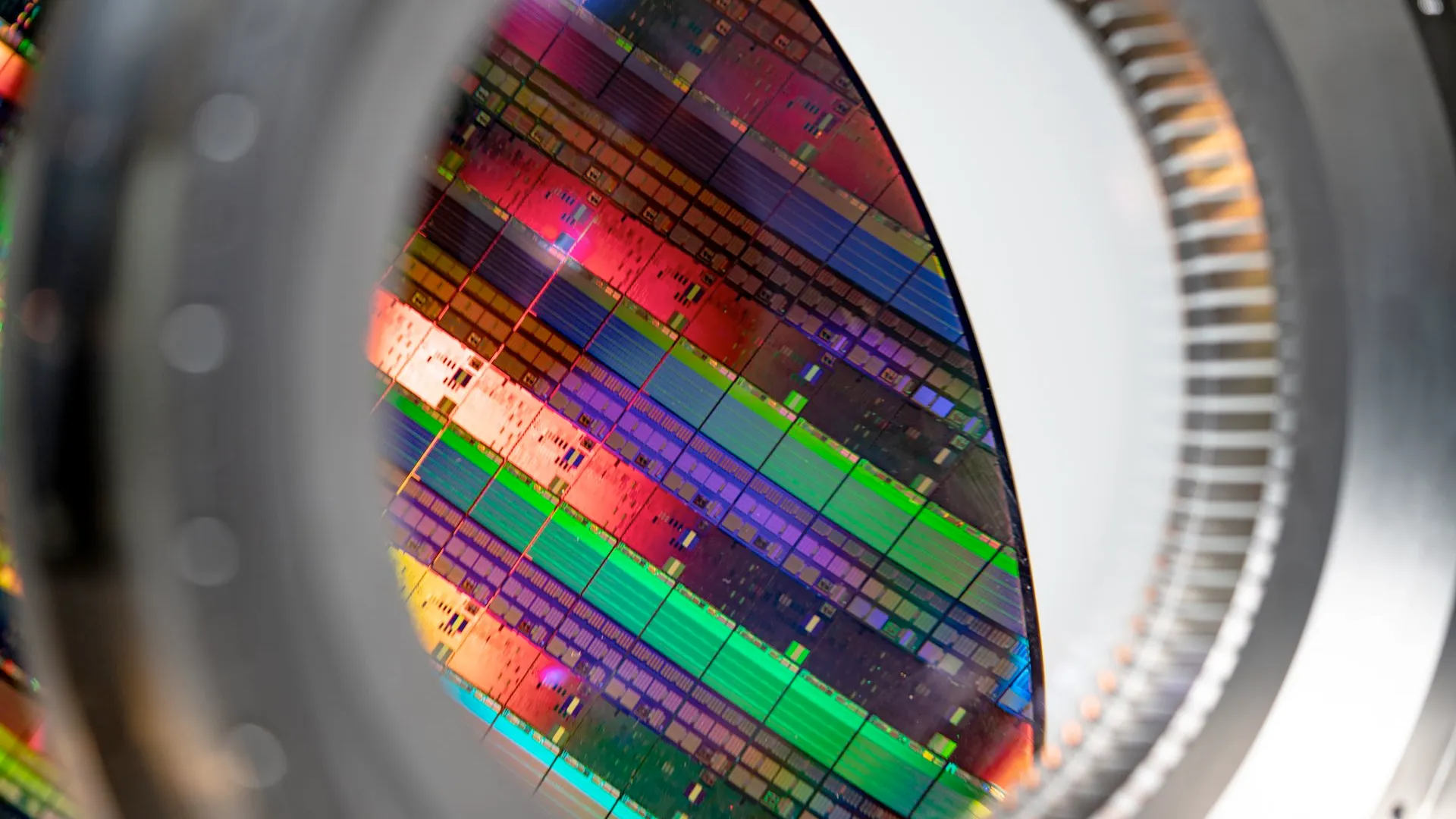
While these measures have worked as intended at the point of sale, they haven’t eliminated the installed base of immersion scanners already operating inside China. Over the past decade, Chinese fabs acquired dozens of high-end DUV tools, which now form the backbone of China’s most advanced production lines, particularly for 14 nm, 10 nm, and experimental 7 nm-class processes that rely heavily on multipatterning. Despite tens of billions in capital expenditure on chipmaking tools, China remains more than a decade behind current market leaders.
Under current rules, ASML is allowed to provide basic maintenance and support to keep these tools running, but it is restricted from performing upgrades that would materially improve performance beyond narrow thresholds. That has created a gap between what the original equipment manufacturer can legally do and what fabs are technically capable of doing with the right parts and expertise.
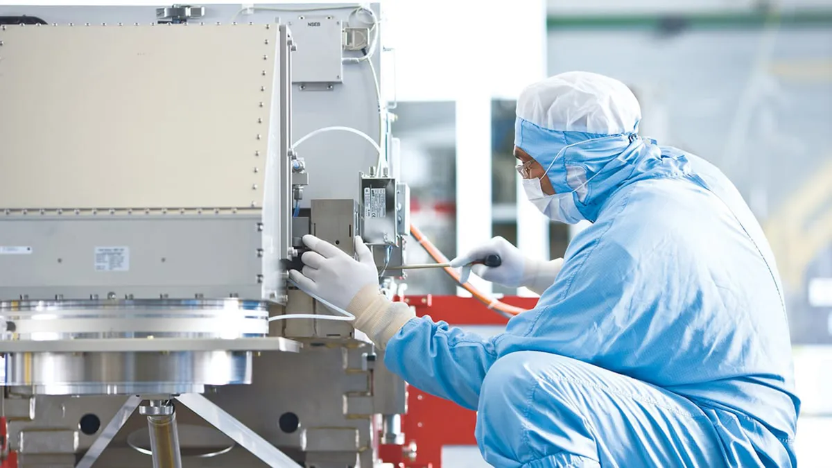
Into that gap has stepped a growing ecosystem of third-party suppliers and engineers. According to the report, Chinese fabs have sourced replacement or upgraded components such as wafer stages, optical elements, sensors, and control subsystems through secondary markets. Some of these parts originate from dismantled tools outside China, while others are produced by suppliers that operate in regulatory grey zones. Installation and calibration work is carried out by independent engineers, including former lithography specialists, rather than by ASML personnel.
This might sound inconsequential on the face of it, but with an outright ban on exports of new tooling, marginal improvements to existing tools compound quickly across high-volume lines. A small improvement in overlay stability can translate into higher yields across dozens of layers.
Overcoming overlay challenges

The primary challenge Chinese fabs will face in upgrading older DUV machines is overlay — the precision with which each new lithography layer aligns with previously-exposed layers. At older nodes, modest overlay errors are tolerable, but not at advanced nodes manufactured without EUV. Multipatterning schemes such as self-aligned double or quadruple patterning dramatically increase the number of exposures required per layer, and each exposure introduces additional misalignment risk.
ASML’s own product pages for the NXT immersion platform make clear how tightly overlay and system stability are linked. Wafer stage accuracy affects not only positioning but vibration and thermal drift, both of which become limiting factors as pattern density increases. Upgrading or replacing these subsystems can claw back some performance that would otherwise be lost to wear and aging. Even without changing the core exposure wavelength or numerical aperture, better stages and sensors can improve effective overlay and reduce the number of wafers scrapped due to misalignment.
This does not eliminate the structural disadvantages of DUV at 7nm-class geometries: Cycle times remain longer than EUV-based processes, costs per wafer are higher, and yields are generally lower. But for products where absolute cost is less critical than domestic supply and technical continuity, these penalties are acceptable.
Limits of enforcement
From a policy perspective, the actions of these firms highlight a shift in which enforcement pressure must be applied to constrain output. Blocking new tool shipments has already occurred, so the harder problem is constraining the flow of parts, expertise, and process knowledge that keeps existing tools competitive — at least for now.
Updates to U.S. BIS rules last year point in this direction, with expanded controls on semiconductor manufacturing equipment components, software, and services. Restrictions increasingly target not only lithography scanners themselves but also metrology tools, process control software, and advanced sensors that indirectly affect yields. The logic is to close the pathways that allow incremental upgrades to accumulate into meaningful capacity gains.
Even so, enforcement potential is limited. Lithography tools are complex systems with long service lives, and many components are designed to be replaceable. Distinguishing between a like-for-like replacement and a performance-enhancing upgrade is technically and legally difficult, particularly when work is performed by third parties rather than the OEM.
China, for its part, seems to be pursuing parallel strategies. Stretching DUV capability through upgrades is one track; developing domestic lithography tools is another. SMIC has tested homegrown immersion DUV prototypes, and state-backed programs continue to fund long-term EUV research, even if breakthroughs remain distant.
At the end of the day, we’re not about to see a sudden leap in Chinese semiconductor capability because a few fabs have upgraded their machines. What we could see, however, is a slower erosion of the gap that export restrictions were designed to maintain.
DUV will continue to significantly lag EUV-based competitors on both cost and efficiency, but they are unlikely to stagnate at their initial performance levels. Incremental improvements in yield and throughput can sustain meaningful volumes of advanced chips for domestic use, particularly in areas such as networking silicon and specialized processors.
