
China injects tens of billions of dollars in chipmaking tools, but it's easily more than a decade behind the market leaders — Here's why
China's attempt to build a self-sufficient semiconductor industry has been instrumental in creating numerous companies, such as Huawei's HiSilicon, SMIC, and YMTC, that develop and manufacture world-class chips. However, while there are China-based firms that produce chipmaking tools, they cannot replace equipment made by American or European companies for advanced process technologies. Some, like Goldman Sachs, believe that China's chipmaking capability is about 20 years behind ASML, but there are signs that the situation may be more optimistic. But can China indeed unbind itself from the leading suppliers of chipmaking tools?
World-class memory and logic on Western tools
Domestically manufactured equipment accounts for just 15% to 30% of the total tools deployed in Chinese semiconductor fabs (according to AMEC estimates), which means that 70% to 85% of the tools they use are procured from American, European, Japanese, or South Korean companies.
Article continues belowTo that end, it is crucial for the People's Republic's semiconductor industry to build its own EDA tools, ecosystem, and wafer fab equipment (WFE) supply chains, which the central government fully understands.
Last year, China began assembling the third installment of its Big Fund with the aim of funding companies producing ultra-pure chemistry or silicon wafers, as well as firms that develop and build chipmaking tools. However, this year it expanded the goal of the $50-billion Big Fund III to EDA and simulation tools. There are multiple ways for China to utilize this money to build advanced fab tools, but this will take time —a valuable asset, given the restrictions imposed on the country's semiconductor sector by the U.S. government.
Strong offerings for everything, but lithography
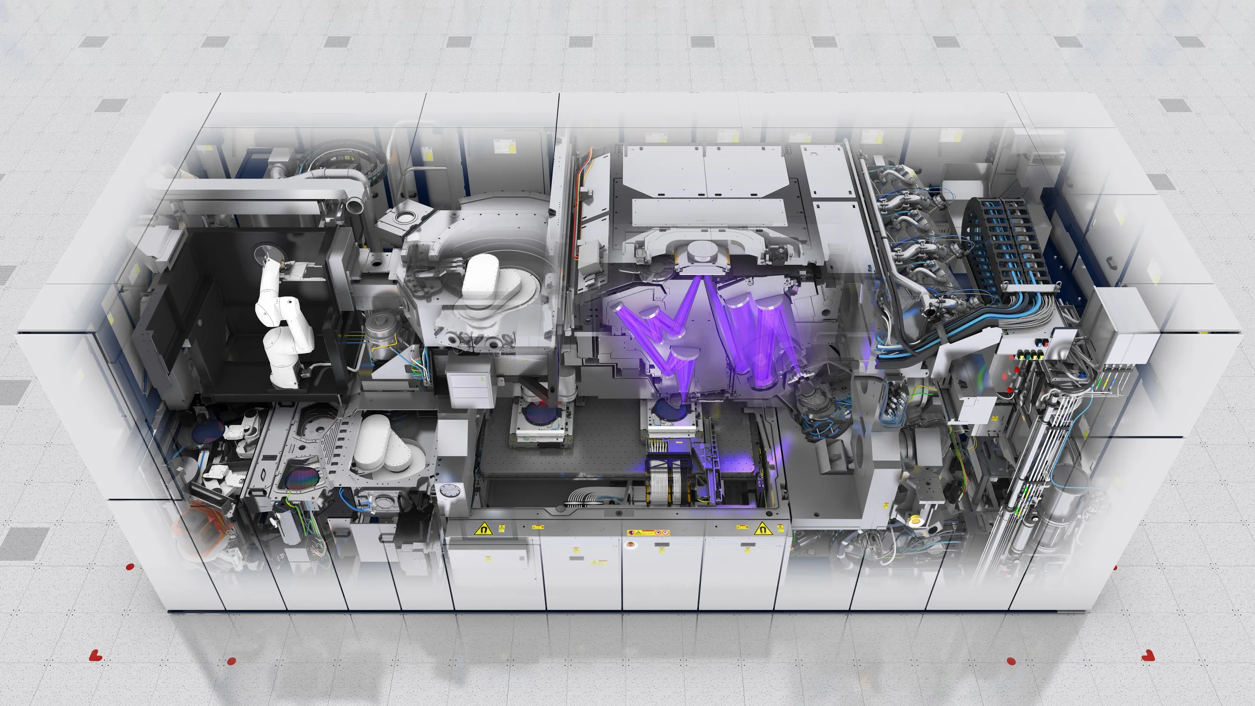
Every semiconductor production facility uses hundreds or thousands of tools, but they can be divided into several groups that perform different steps, including deposition (CVD, ALD, PVD), lithography (including tracking tools and lithography scanners), etching, ion implantation, annealing, cleaning, metrology, and inspection.
China has dozens of companies developing and producing wafer fab equipment for a variety of steps of the front-end production flow (actual semiconductor manufacturing), as well as companies making tools for back-end production (chip packaging).
It is simultaneously good and bad that China has so many WFE companies: on the one hand, there is competition both in terms of products and in terms of ideas, but on the other hand, small companies can't compete against industry giants like Applied Materials or Tokyo Electron. Still, there are quite big firms as well. Perhaps the best-known companies are ACM Research (equipment for cleaning, polishing, electrochemical plating, and plasma-enhanced CVD), Advanced Micro‑Fabrication Equipment (AMEC, deposition tools), Hwatsing Technology (chemical mechanical planarization/polishing), Kingsemi (spin-coating and developing tools), Naura Technology (etching, annealing, etc.), Shanghai Micro Electronics Equipment (SMEE, lithography tools, metrology, inspection tools), Piotech (deposition tools), and YuweiTek (optical inspection and metrology).
SiCarrier is a rising star in China's semiconductor equipment landscape. The company presented a catalog of dozens of fab tools at Semicon China this year and is believed to be developing a full stack of wafer fab equipment from deposition and lithography all the way to annealing and inspection. The main investor of SiCarrier is Shenzhen Major Investment Group, a government-backed fund supporting other semiconductor ventures associated with Huawei, which is why many observers think that SiCarrier is essentially a chipmaking tool arm of Huawei.
For now, Chinese companies have strong local offerings in etching, deposition, cleaning, CMP, and coating/developing, especially for mature and legacy process technologies (e.g., 28 nm and above). In fact, AMEC's tools can be used for the production of chips on 5nm-class nodes, according to the company. However, there is a caveat: many of the WFE equipment made in China uses components from Western companies, which are either subject to export controls already or will become so shortly. What is no less important is that lithography remains the most critical choke point for the People's Republic.
20 years behind?
Designing lithography tools is extremely challenging, as they sit at the intersection of optics, precision engineering, control systems, and materials science, all operating at nanometer-level tolerances in modern fabrication technologies.

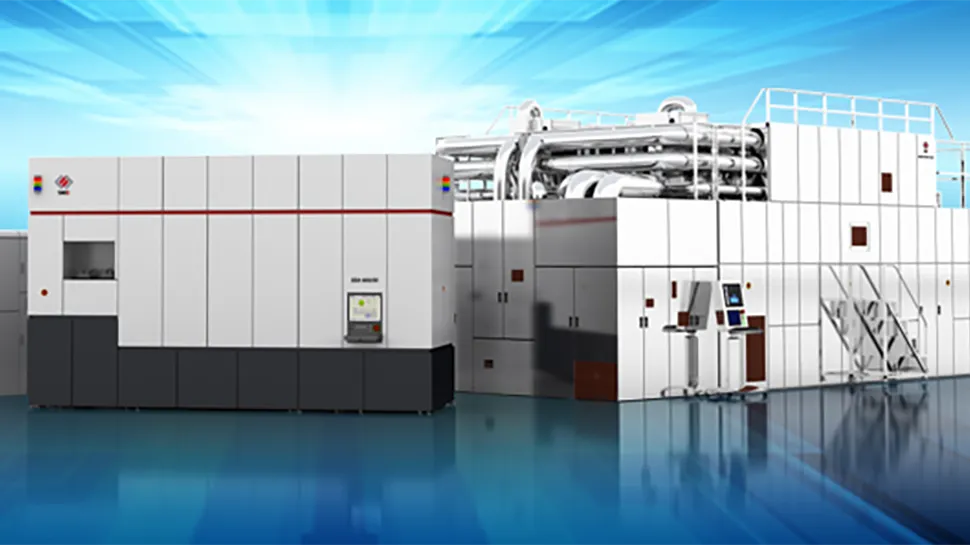
SMEE, China's most advanced maker of litho tools, is significantly behind global leaders like ASML or Nikon. The company formally introduced its 28nm-capable immersion ArF DUV SSA/800-10W litho machine in late 2023, but it still does not list it on its website, and it is unclear whether it has shipped any production tools to actual chipmakers, such as HuaHong or SMIC, which have vast 28nm-class capacities. According to SMEE's website, the best lithography systems it has are the SSA600-series dry scanners, capable of 90nm, 110nm, and 280nm process technologies, which are from the early to mid-2000s.
SiCarrier is also developing lithography machines capable of 28nm-class production nodes (according to a Nikkei report), but the catalog from Semicon did not include any lithography tools, perhaps to keep its lithography developments a secret from the U.S. government, as they heavily rely on components made outside of China.
Keeping in mind that both SMEE and SiCarrier have so far developed lithography systems capable of producing chips on a 28nm-class process technologies, it is safe to say that both companies have managed to build immersion DUV scanners, which is a major milestone. ASML has 5nm-capable immersion DUV machines, which pretty much shows the immense capability of this technology.
However, as the best thing listed on SMEE's website is its dry SSA600-series litho system, comparable to ASML's machines from the early 2000s, analysts from Goldman Sachs have every right to say that SMEE is 20 years behind ASML. But can SMEE and/or SiCarrier leapfrog from a 28nm-capable machine that they cannot ship in volume, to something more advanced? Let's theorize.
Immersion DUV lithography is hard
Modern ArF immersion DUV lithography tools are incredibly difficult to design because they must enable a resolution sufficient for 5nm-class (and possibly beyond that) process technologies using 193 nm-wavelength light, which is far beyond the natural resolution limit of that wavelength.

To overcome this, immersion DUV scanners rely on high numerical aperture (NA) lenses made from ultra-pure calcium fluoride (CaF₂), polished to sub-nanometer surface roughness. ASML claims that only a few companies worldwide have the capability to manufacture optics of this precision, and its advanced tools almost exclusively use optics from Zeiss. Chinese companies do not have access to Zeiss's optics.
Additionally, ArF immersion scanners incorporate a thin layer of high-purity water between the lens and the wafer to enhance resolution. This requires maintaining a 1 mm fluid layer flowing at speeds of up to 1 m/s with no bubbles, turbulence, or contamination, which demands precision control over fluid dynamics and thermal stability.
Mechanical components must match optical precision: the wafer and reticle stages move at high speed but must maintain sub-nanometer accuracy using air bearings or magnetic levitation and have feedback systems that operate at microsecond latency to correct any drift or vibration. Software and sensors must act with a nanometer overlay error, as any deviation in alignment, stage motion, or temperature can destroy the pattern.
Not all mechanical components that ASML uses in its lithography, metrology, or inspection machines are built by the company; many are produced by third parties, so other companies can procure and use them as well (which is how Chinese companies obtain loads of components for their WFE). However, replicating ASML's software and firmware is as challenging as assembling a high-precision machine.
Chinese firms like SMEE, attempting to develop similar immersion DUV systems (like the SSA/800‑10W), must not only replicate the success in the face of extreme engineering challenges, but also replace or recreate every banned or restricted component from scratch. This is why even reaching 28nm-class capability is considered a major milestone.
However, moving to 16nm or 7nm is not a linear progression for ASML or SMEE, so it does not get meaningfully easier. In fact, the jump from 28nm to 7nm lithography involves entirely new classes of technology, control, and precision, with exponentially higher complexity and capital intensity. Technologies involved in ASML's latest DUV scanners are protected by various export controls (which prohibit shipping technologies enabling Chinese entities to make 16nm-class (and below) logic chips to China), so essentially, SMEE cannot get any help from the outside world.
ASML's 28 nm-class DUV capability (via Twinscan XT:1930i/1950i) was mature around 2010, whereas its DUV-based 5 nm-class capability using self-aligned quadruple patterning (SAQP), complex optical proximity correction (OPC), new masks, and new resists (among other things, of course), was commercially supported by 2020 with the Twinscan NXT:2000i. Nikon began sales of its 7nm-capable NSR-S636E in early 2024.
SMEE yet has to achieve maturity with its SSA/800-10W and produce it in high volume before attempting to move towards 16nm and 7nm. Considering that virtually no newly built fabs in China target 28nm technologies and below, it is unlikely that SMEE is close to volume production of its SSA/800-10W. As a result, SMEE is probably over 10 years behind ASML's NXT 2000i, and well over 15 years behind ASML's contemporary EUV tools (we are not going to touch upon EUV in this article because it is a completely different branch of technology development that requires plenty of innovations that took 20+ years).
No domestic tools for advanced nodes in the next 10 or more years
There is no way that SMEE or SiCarrier can make semiconductor breakthroughs faster than ASML did, so you shouldn't expect either company to come up with a 7nm or 5nm immersion DUV scanner in less than 10 years. While industry espionage and reverse engineering of tools that Chinese companies already have can speed up some developments, replicating ASML's Twinscan NXT:2000i is impossible not only because it has 100,000+ bleeding-edge parts, but also because the process will require replication of the entire ecosystems behind this machine.

As there are no shortcuts that can lead to NXT:2000i-class machines, SMEE and SiCarrier have to invest billions in internal R&D, master their optical and precision mechanic capabilities, work closer with third parties to develop new classes of raw materials and parts, and cooperate with fabs to take into account their developments.
In short, while China's semiconductor industry may achieve self-sufficiency with mature nodes in the coming years and perhaps even produce world-class tools for deposition, etching, ion implantation, annealing, and cleaning, there is no way that Chinese companies can catch up with ASML or Nikon in lithography any time soon. To that end, China will have to rely on advanced lithography tools for 7nm or 5nm-class technologies made in Europe or Japan for the next 10 years at least.
