Shanghai Micro Electronics Equipment Group (SMEE), a Chinese developer of lithography tools, announced its first machine capable of processing wafers using a 28nm-class process technology, reports Bloomberg. This advancement represents a major leap in China's quest to close the technological gap in the global chip industry. The device is still behind tools made by market leader ASML, however, and it is unclear when SMEE can produce these scanners in significant volume.
The announcement did not come without oddities. The news about this new litho machine was first shared by Zhangjiang Group, a state-backed company that controls SMEE's fourth-largest shareholder, in a WeChat post that sent its shares up by 8%. But after that, the company changed its post and removed any mentions of the 28nm-capable tool, focusing on the fact that SMEE was committed to building advanced lithography machines. This is a bit surprising as SMEE said in October that it would introduce a 28nm-capable lithography tool by the end of the year.
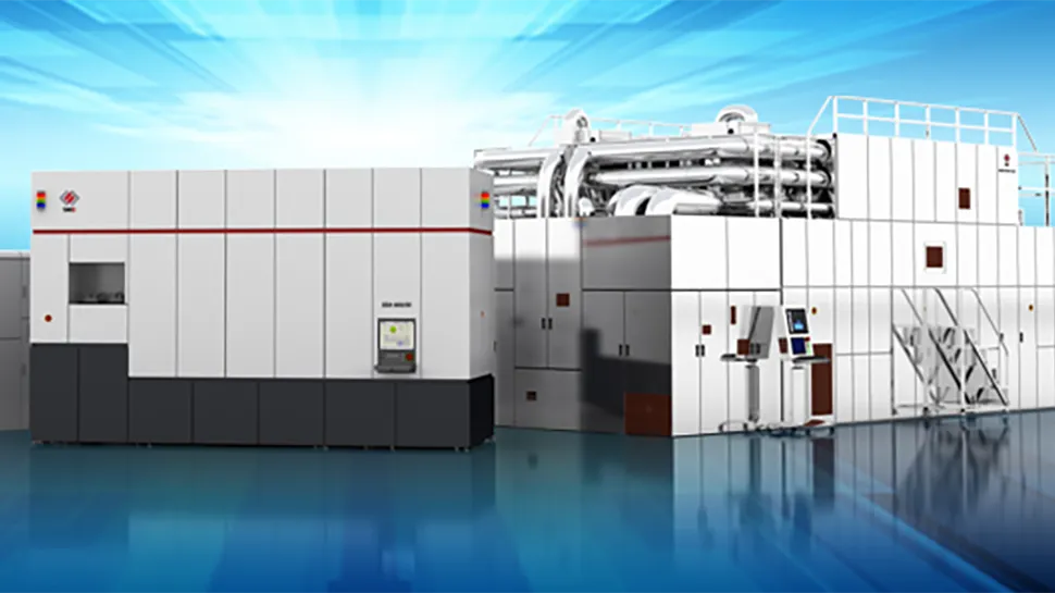
The scanner is reportedly called SSA/800-10W and represents a major breakthrough for the company; its existing SSA600-series machines are capable of 90nm, 110nm, and 280nm process technologies.
TSMC has been producing chips on its 28nm process technology since 2011, whereas China's SMIC adopted a similar technology in 2015. Both SMIC and TSMC have used ASML's litho tools to make appropriate chips.
It's the latest development in a tit-for-tat chip war pitting the United States against China: The latest export rules set by the U.S. government block Chinese chip manufacturers from acquiring the necessary equipment and know-how to produce advanced non-planar transistor logic chips smaller than 14nm/16nm, 3D NAND chips with more than 127 active layers, and DRAM ICs with a half-pitch under 18nm.
Additional restrictions from the Netherlands, Japan, and Taiwan, which came into effect earlier this year, have further cut off Chinese companies from sophisticated tools. These constraints hinder their ability to fabricate chips using their latest manufacturing nodes, particularly SMIC's 14nm/12nm and second-generation 7nm processes and YMTC's 128-layer and 232-layer 3D NAND chips. Meanwhile, the U.S. Department of Commerce put SMEE into its Entity List last year, trying to stop China from advancing its semiconductor industry with its own tools.