China's First 28nm Lithography Tool to Be Delivered This Year

SMEE
(Image credit: SMEE)

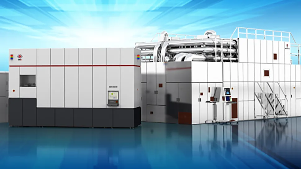
Shanghai Micro Electronics Equipment (SMEE), China's most successful lithography scanner manufacturer, reiterated plans this week to deliver its first scanner capable of producing chips on a 28nm-class fabrication process by the end of the year, reports TechWire Asia, citing newspaper Securities Daily, which in turn cites an unnamed source.

For SMEE, its SSA/800-10W scanner is a breakthrough since the most advanced scanner that the company has today is only capable of 90nm and thicker fabrication processes. A 28nm-capable lithography tool will over time enable Chinese chipmakers to rely on domestic lithography equipment for a range of mature technologies.

The move is part of China's broader goal to achieve semiconductor self-sufficiency and reduce its dependence on foreign technology. But the question remains as to whether SMEE can produce this scanner in mass quantities, and when it can make such scanners available to substitute for machines from ASML, Canon, and Nikon.

The latest export regulations from the U.S. government prevent Chinese chipmakers from accessing tools and technologies essential for creating non-planar transistor logic chips under 14nm/16nm dimensions, 3D NAND chips with over 127 active layers, and DRAM ICs with a half-pitch smaller than 18nm. Restrictions from the Netherlands, Japan, and Taiwan that went into effect earlier this fall further isolated Chinese firms like SMIC and YMTC from advanced tools. These limitations impede their ability to produce chips using their newest manufacturing processes, notably SMIC's 14nm/12nm and 2nd generation 7nm as well as YMTC's 128-layer and 232-layer 3D NAND.

As a result, China needs advanced domestic lithography tools to ensure that its chipmakers can produce chips on even fairly advanced process technologies, such as 14nm. For now, it looks like Shanghai Micro Electronics Equipment is on track to reveal its 28nm-capable SSA/800-10W scanner, which it will ship either to SMIC or a chip research intitute.

After it does this, it will still take some time for the chipmaker to integrate the new scanner into its production flow. However, it will only do this only if SMEE can produce a sufficient number of such tools.

Anton Shilov
Freelance News Writer

Anton Shilov is a Freelance News Writer at Tom’s Hardware US. Over the past couple of decades, he has covered everything from CPUs and GPUs to supercomputers and from modern process technologies and latest fab tools to high-tech industry trends.

  • ThomasKinsley
    I am a little confused about the nm class of these machines. China has been using DUV lithography (sources say 254–193-nm wavelength of light) to produce chips. Some reports claim they are able to use these machines to produce chips as small as 7nm. Is this 28nm-class scanner capable of producing smaller components or is it strictly capable of producing at 28nm?
    Reply
  • TCA_ChinChin
    ThomasKinsley said:
    Is this 28nm-class scanner capable of producing smaller components or is it strictly capable of producing at 28nm?
    Good question, I'm also curious and have no idea.
    Reply
  • cyrusfox
    ThomasKinsley said:
    I am a little confused about the nm class of these machines. China has been using DUV lithography (sources say 254–193-nm wavelength of light) to produce chips. Some reports claim they are able to use these machines to produce chips as small as 7nm. Is this 28nm-class scanner capable of producing smaller components or is it strictly capable of producing at 28nm?
    193nm immersion scanners can natively create 36nm with no multi-patterning tricks, with multi-patterning you can halve that (Known as pitch doubling, or even pitch quad, or any of various multiple industry terms), single application of this will enable print size of ≈18nm at the expense of additional processing steps (that come with added defects and error propagation). if you apply multipattern multiple times you can achieve sub 10nm. Not sure anyone has done more than a 2x cycle of this as it is quite cost prohibitive and errors multiply. I expect this scanner is only able to achieve 28nm class performance with multi-patterning or they are twisting logic and printing 36nm lines and calling it 28nm class.

    If you want to know how good US semi fabs got at patterning, look at 2D Planar fab shrinkage which was actually accurate on marketing, IE true resolution unlike the current TSMC/Intel/Samsung Logic marketing terms. For NAND it was continously verified by actual chip teardowns/deprocessing.
    2D NAND ran in to scaling issue, hence the change to stacking/3D. Any tech becomes more costly to go smaller (multiple patterning tricks vs EUV) and NAND memory cells degrade as you go smaller, playing with smaller number of electrons leading to less cycles before failure with each subsequent shrink. Hence all NAND players transitioned to 3D stacking after they got as much performance as possible from the 14-16nm range.
    Reply
  • cyrusfox
    This is impressive, if China is cost competitive here, they could provide competition to aging scanner tech in the US, we could see China litho tech in the USA in the future going against aging Nikon, Canon, and old ASML immersion tech. Still a lot of semi work done larger than 10nm out there.
    Reply
  • Amdlova
    China making cheap stuff is good for everyone.
    Reply
  • The Historical Fidelity
    Amdlova said:
    China making cheap stuff is good for everyone.
    ahh yes, like the lead painted children’s toys and formaldehyde releasing building materials. You’re right, cheap Chinese stuff is good for everyone!
    Reply
  • TCA_ChinChin
    The Historical Fidelity said:
    ahh yes, like the lead painted children’s toys and formaldehyde releasing building materials. You’re right, cheap Chinese stuff is good for everyone!
    You forgot iPhones and everything else China makes. When you pay for cheap, you get cheap.
    Reply
  • vehekos
    28 nm is 20 years old technology.

    But processors didn't advanced much in 20 years.
    Reply
  • cyrusfox
    vehekos said:
    28 nm is 20 years old technology.

    But processors didn't advanced much in 20 years.
    28nm did not ramp until 10 years ago...
    Figure 1: Advanced technology capacity, 28 nanometer and below (includes 32-nanometer)Westmere and Sandy Bridge (32nm) come from this level of technology, Sandy Bridge brought a huge uplift to Core performance.

    If these reports are accurate it is impressive what China is achieving this against the western semiconductor embargoes. 28nm is the sweet spot for economical fabrication (no EUV and don't need to multi-pattern). Covid showed an extreme shortage of chips that is already heavily located in Asia. If China makes this cheap enough they can further corner the market on generalized semiconductors.

    It appears to me that all the chip money is going towards making new shiny high margin products, not the bulk of IC that are needed like the simple analog and digital devices, 1 to 10 cent pieces, the semiconductor commodity market that long ago left our shores. I don't see any of this chip money from the US or European governments being used to return that side of supply back to the west. China and Asian in general will still be a critical side of the supply as many of these commodities will never be profitable to produce in the west.
    Reply
  • The Historical Fidelity
    cyrusfox said:
    28nm did not ramp until 10 years ago...
    Figure 1: Advanced technology capacity, 28 nanometer and below (includes 32-nanometer)Westmere and Sandy Bridge (32nm) come from this level of technology, Sandy Bridge brought a huge uplift to Core performance.

    If these reports are accurate it is impressive what China is achieving this against the western semiconductor embargoes. 28nm is the sweet spot for economical fabrication (no EUV and don't need to multi-pattern). Covid showed an extreme shortage of chips that is already heavily located in Asia. If China makes this cheap enough they can further corner the market on generalized semiconductors.

    It appears to me that all the chip money is going towards making new shiny high margin products, not the bulk of IC that are needed like the simple analog and digital devices, 1 to 10 cent pieces, the semiconductor commodity market that long ago left our shores. I don't see any of this chip money from the US or European governments being used to return that side of supply back to the west. China and Asian in general will still be a critical side of the supply as many of these commodities will never be profitable to produce in the west.
    Uhh, I live right next to Texas Instruments, one of the biggest analog and digital IC makers in the world…
    Reply