American startup Substrate promises 2nm-class chipmaking with particle accelerators, at a tenth of the cost of EUV — X-ray lithography system has potential to surpass ASML's EUV scanners
If it can build a fab to match its tool.
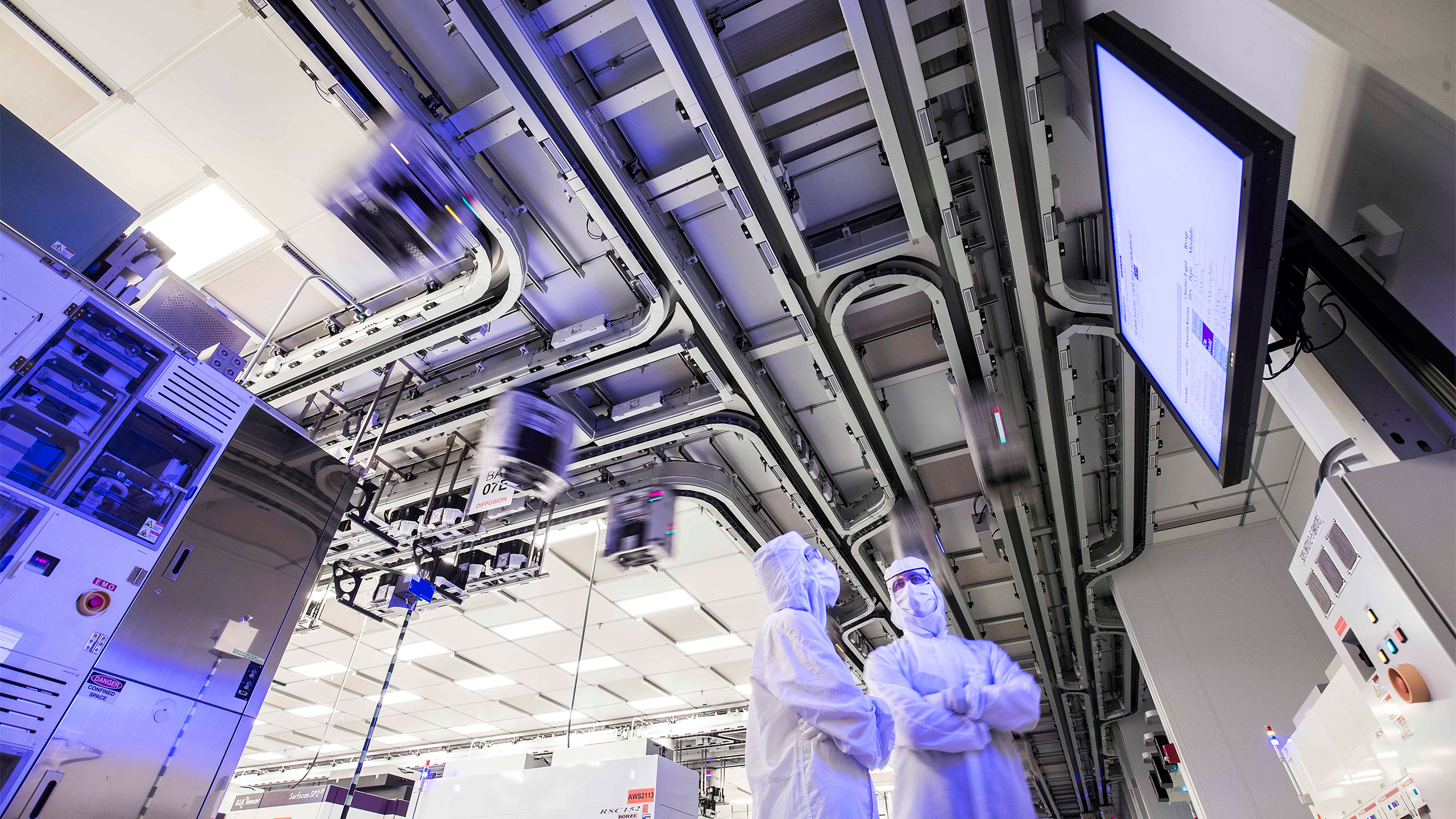
Get Tom's Hardware's best news and in-depth reviews, straight to your inbox.
You are now subscribed
Your newsletter sign-up was successful
This free-to-access article was made possible by Tom's Hardware Premium, where you can find in-depth news analysis, features, and access to Bench. Subscribe now from just $7 per month for a limited time.
American startup Substrate is developing a new X-ray lithography (XRL) system, powered by a particle accelerator-based light source, that promises superior performance and cost efficiency compared to standard EUV lithography, aiming to achieve resolutions equivalent to ASML's 2nm-class processes. The firm also claims it can advance beyond that. Substrate also claims that its efforts will be cheaper to produce than the competition's and will offer finer resolutions before 2030, as the company detailed on its website.
However, the tool that Substrate is developing does not appear to be compatible with existing equipment and production flows, so the company will have to reinvent the whole supply chain to be successful. However, Substrate does not plan to sell its tool, but to build its own fab and provide foundry services.
Expensive tools = expensive chips
As integrated circuit features are getting smaller, chipmakers are using increasingly intricate lithography tools that now cost around $235 million for an ASML NXE:3800E Low-NA EUV scanner or around $380 million for an ASML EXE:5200B High-NA EUV scanner. As a result, fabs are becoming increasingly expensive to build, and chips are becoming more expensive to produce.
Article continues belowSubstrate models that a leading-edge fab will cost around $50 billion by 2030, leaving semiconductor production to a handful of companies with very deep pockets. Furthermore, such fab expenditures are expected to increase the cost of a 300-mm wafer, which it claims could balloon to $100,000 when using leading-edge fabrication processes. This will make the development and production of advanced chips prohibitively expensive for small companies. Substrate intends to change that and reduce wafer pricing to just $10,000 by 2030.
"At Substrate, we have a pathway to reduce the cost of leading-edge silicon by an order of magnitude compared to the current cost-scaling path we are on," a statement by the company reads. "By the end of the decade, Substrate will produce wafers closer to $10,000, not $100,000."
Note that Substrate is by no means the only company exploring particle accelerators as light sources for EUV or beyond-EUV lithography. In the U.S. alone, two companies — Inversion Semiconductor and xLight — as well as researchers at Johns Hopkins University, have revealed that they are working on lithography systems harnessing particle accelerators over the past 12 months. Chinese scientists and Japanese researchers are also testing particle accelerators for semiconductor production.
Substrate's X-ray lithography
Substrate is developing a new type of lithography system that uses a particle accelerator to produce short-wavelength X-ray radiation (or light) for chipmaking. The goal is to replace ASML's expensive EUV lithography scanners with compact, low-cost machines capable of printing transistor patterns at a 2nm-class process technology (or even more advanced, the company claims). The firm claims the machine should reduce chip production costs by 10 times by the end of the decade.
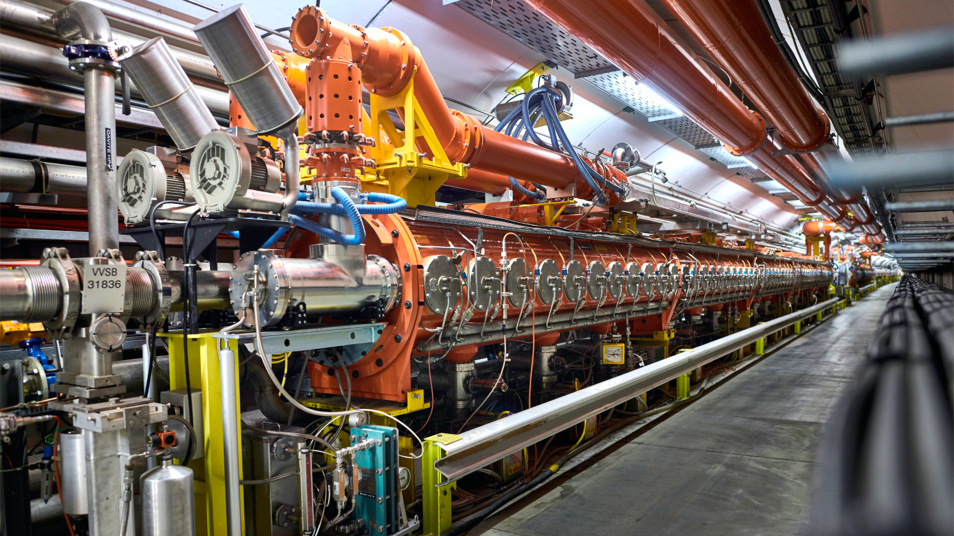
At the core of Substrate’s technology is a custom particle accelerator which propels electrons (produced by an unknown emitter) to near the speed of light using radio-frequency cavities. As these electrons pass through sporadic magnetic fields, they gain kinetic energy, accelerating to speeds very close to the speed of light (a relativistic speed), which allows them to produce special types of light when manipulated. These fast-moving electrons fly through a series of magnets that flip back and forth, wiggling the electrons and causing them to release their energy and produce coherent bursts of intense X-ray light (or radiation).
That light is 'billions of times brighter than the sun,' likely producing pulses intense enough to achieve the desired resolution and dose. The X-ray pulses are then focused by 'a succession of perfectly polished optics' to project a photomask onto a photoresist-coated silicon wafer. Note that Substrate never mentions reticle and resist in its official description, only claiming that 'bright pulses of light' are collimated and transported 'all the way to the silicon wafer,' which implies maskless direct-write lithography, which is good enough for research purposes, but orders of magnitude too slow for the mass production of chips. However, this remains speculation on our part.
In fact, Substrate's description of its technologies is very brief and lacks detail (perhaps for competitive reasons), making it difficult to analyze. However, since the company mentions X-ray, we are dealing with electromagnetic radiation with wavelengths ranging from 0.01nm to 10nm and energies from about 100 eV to 100 keV. The shorter the wavelength, the finer the structure that can the printed with improved accuracy, but the harder the light is to manage and work with.
Given Substrate's achievements so far, we are likely dealing with soft X-rays (wavelengths of 1-10 nm, lower energy) rather than hard X-rays (wavelengths of 0.1-1nm, higher energy).
Since short-wavelength light (including EUV and X-rays) is strongly absorbed by most materials, managing it requires a set of perfectly polished mirrors that reflect light at grazing angles (to avoid absorption), ultra-precise alignment, and vacuum environments. Also, X-ray lithography requires all-new resists that can handle high-energy photons without damage or blur.
Achievements so far
2nm-like CD and T2P spacing
To prove that its XRL method works, Substrate has shown off images of a random logic contact array with 12nm critical dimensions (CD) and 13nm tip-to-tip (T2T) spacing printed with high pattern fidelity, as well as random vias with a 30nm center-to-center pitch, possessing superb pattern quality and critical dimension uniformity. If such metrics could be achieved for mass production today, this would largely revolutionize the lithography industry, as it would enable scaling across both axis at 2nm-class nodes (and lower) without using multi-patterning.
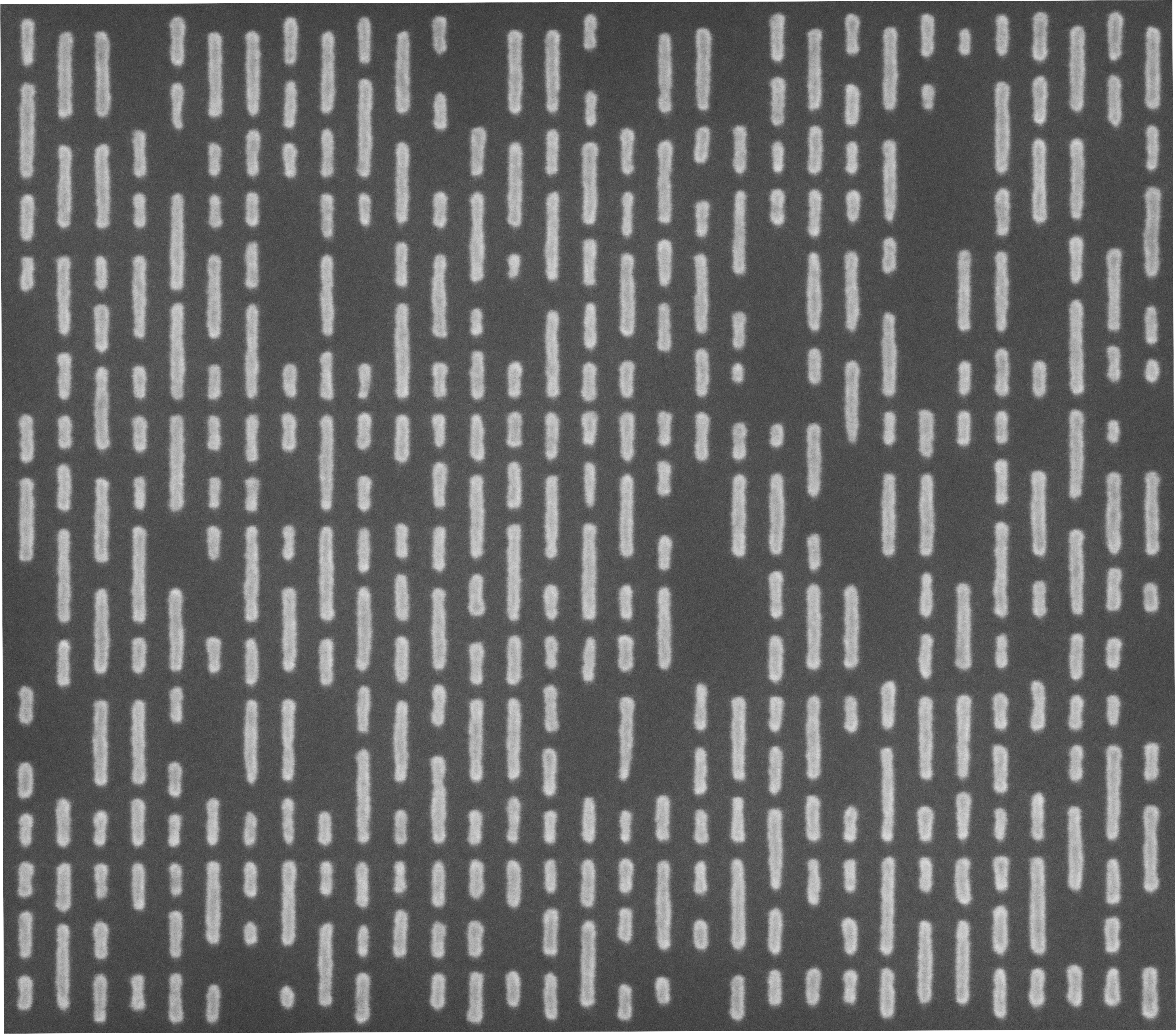
Modern EUV scanners with 0.33 NA optics can achieve critical dimensions of 13nm–16nm in high-volume manufacturing, which is sufficient to print a 26nm minimum metal pitch (good enough for 2nm or 3nm-class process technologies) and a 25nm T2T interconnect space with a single exposure.
Such disproportions emerge because chipmakers tend to optimize resolution in the Y direction (CD) to get the tightest metal-pitch line-space pattern, but at the cost of resolution in the X direction, which means that T2T prints poorly or inconsistently, leading to bridging defects, stochastic defects, yield loss, complicated design rules, and slower scaling. To mitigate this and avoid blurred or inconsistent line ends at tip-to-tip spacing, Intel applies pattern-shaping tools in the X-direction with its 18A fabrication technology, but this complicates the overall production flow and does not fundamentally solve the issue.
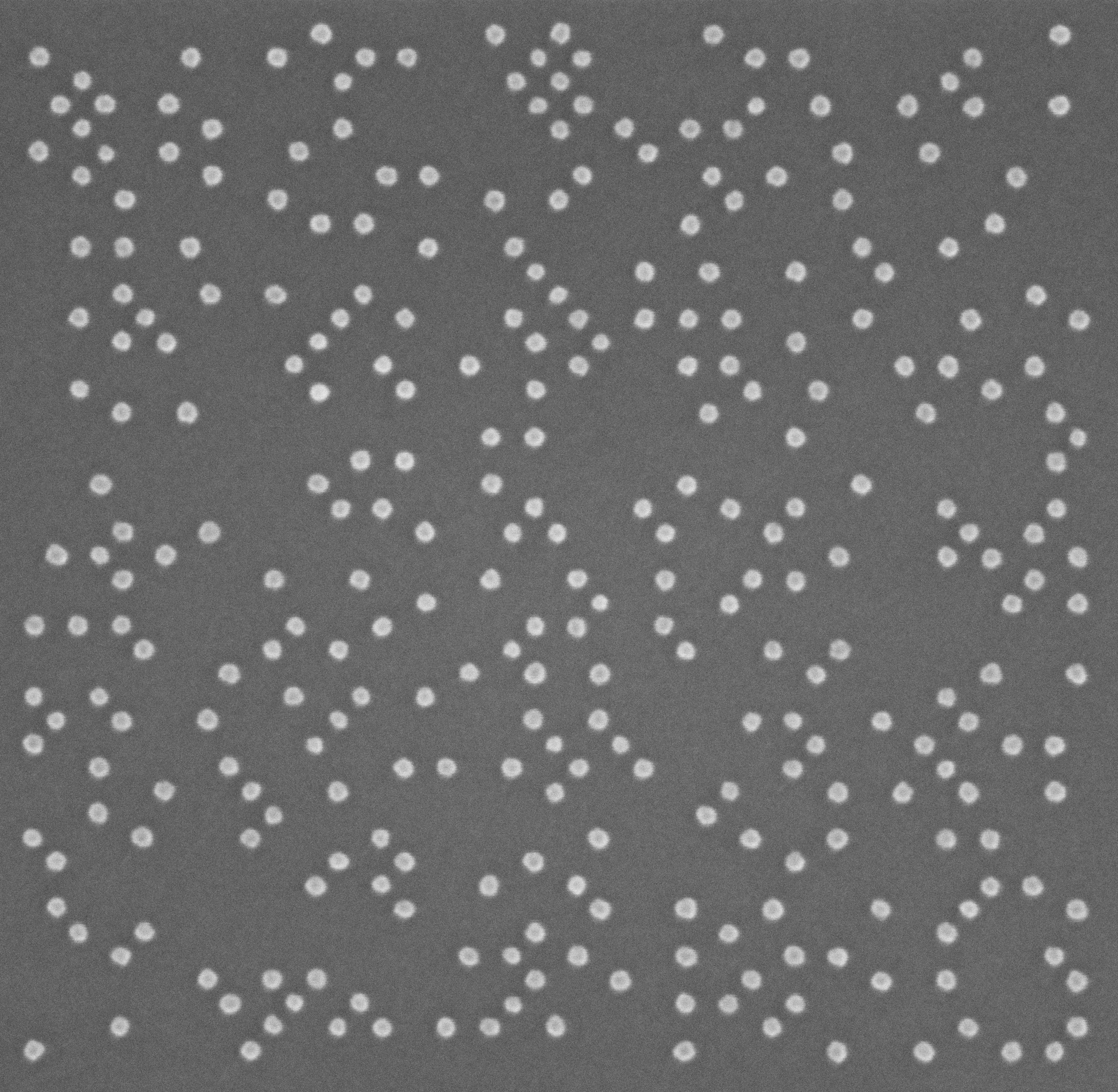
Substrate's tool (assuming these are real lab results, not a simulation) can already outperform existing Low-NA EUV scanners in terms of achievable CDs with single-resolution patterning, and it leaves them behind dramatically when it comes to T2T spacing printed with high fidelity. This means that Substrate's X-ray lithography tool could possibly replace costly EUV multi-patterning used for sophisticated 3nm and 2nm-class process technologies or pattern shaping used for Intel 18A.
Our friends at SemiAnalysis have managed to get more performance claims from Substrate, which look even more impressive. The company claims it has achieved overlay accuracy of under 1.6nm, full wafer critical-dimension uniformity (CDU) of 0.25 nm, line edge roughness (LER) of under 1nm, and local critical dimension uniformity (LCDU) below 1.5 nm.
If accurate, this performance would match or surpass ASML's Twinscan NXE:3800E in uniformity, though its overlay precision is slightly worse than the 0.9nm machine-matched overlay standard in the latest EUV scanners. Also, the line-width uniformity of contacts on an image provided by Substrate is rather poor.
Assuming the results presented by Substrate are real and achieved in a lab environment, this means the company has solved three critical challenges with X-ray lithography. First, build a light source featuring an electron gun and a particle accelerator; second, create a grazing-incidence mirror system to reflect and focus X-rays at very shallow angles; and make the whole thing compact enough to fit into a lab.
Future challenges
However, Substrate still has a lot of work to do, turning its X-ray lithography technology from a lab success into a viable production tool. Substrate must prove that its X-ray lithography system can maintain beam stability, optical precision, resist compatibility, overlay accuracy, and commercial throughput simultaneously, something no X-ray platform has ever achieved.
Existing photoresists are incompatible with X-ray radiation, as they are optimized for EUV radiation with considerably lower photon energy. So, Substrate will have to invent a proper resist and then produce it at volume. The company will also have to develop photomasks that can sustain X-ray radiation. Grazing-incidence mirrors for X-rays are also not in mass production, and it is unknown whether they can be mass-produced cheaply and reliably by existing producers like Zeiss.
Substrate will also have to ensure that X-rays do not damage the underlying transistors or introduce stochastic defects. Achieving overlay accuracy below 1nm (to match ASML's production-level alignment precision) remains another challenge for the company. This is perhaps because the company still has to address issues such as wafer handling, stage repeatability, and other factors related to high-precision mechanics, which ASML has taken decades to solve.
Beyond that, the tool must reach commercial throughput and consistent yield, something that took years for ASML's EUV tools. In fact, ASML's EUV journey timeline is quite exemplary: it has taken the industry 12 years to evolve from an alpha demo tool (2006) to mass production (2018), and about seven years to go from the first pre-production system (2010) to a mass-production-capable scanner.
A new paradigm
Speaking of mass-production-capable X-ray lithography tools, it is important to note that Substrate has no intention of selling them to third parties such as Intel or TSMC. Instead, Substrate plans to build its own fabs in the U.S. (a move that could give the company geopolitical importance in the eyes of the U.S. government), install additional tools, and offer foundry services, thus challenging existing chip contract manufacturers.
However, this strategy adds complexity and cost. Constructing even a single high-end semiconductor fabrication plant would require tens of billions of dollars in investment and a large ecosystem of suppliers and service infrastructure, which currently does not exist for X-ray lithography production.
Substrate would also need to integrate its XRL litho machines with hundreds of other tools in the fab, or persuade its suppliers (such as Applied Materials, KLA, Lam Research, etc.) to help it do so, which likely involves further investments from the company, making its first fab particularly expensive.
Also, running both a toolmaking activity and a chip foundry would stretch Substrate's technical and financial resources, which would make it particularly hard to achieve its promised per-wafer price of $10,000 by the end of the decade, as its investors will likely demand returns after pouring tens of billions of dollars into the company.
However, if Substrate succeeds in both roles, it could shift the balance of the semiconductor supply chain back to the U.S., as the company will likely outpace ASML's tools in terms of resolution and performance, and TSMC in terms of design cycle time and potentially volume.
To get more insightful news analysis, Subscribe to Tom's Hardware Premium from just $7 per month for a limited time.

Follow Tom's Hardware on Google News, or add us as a preferred source, to get our latest news, analysis, & reviews in your feeds.
Anton Shilov is a contributing writer at Tom’s Hardware. Over the past couple of decades, he has covered everything from CPUs and GPUs to supercomputers and from modern process technologies and latest fab tools to high-tech industry trends.
-
bit_user Is this the same startup that Gelsinger was previously talking about? Or was that someone just building more compact EUV light sources?Reply
@thestryker ? -
thestryker Reply
No, the company he's involved with is xLight.bit_user said:Is this the same startup that Gelsinger was previously talking about?
Augmenting existing EUV machines is what xLight is doing. I'm not sure how much smaller their light source would be, but I know they're aiming at more powerful and efficient which would be huge.bit_user said:Or was that someone just building more compact EUV light sources? -
supreem 'Particle accelerator'. Technically right but it's literally just producing X-ray. The title make it as if they're using electron beam or something for patterning and exposureReply -
edzieba Reply
Yep, they managed to write several paragraphs about Free Electron Lasers without actually mentioning Free Electron Lasers. Extra confusion, as particle-beam lithography is its own separate thing that isn't relevant here. making the headline actively misleading.supreem said:'Particle accelerator'. Technically right but it's literally just producing X-ray. The title make it as if they're using electron beam or something for patterning and exposure
FELs can generate any wavelength of EM radiation (within the bandwidth of your electromagnet array), so could be used as EUV - or DUV for that matter - light sources too. They are not, because their efficiency is so astonishingly low that the current vaporised-tin-drop method of EUV generation is still a superior option. -
usertests Reply
The opposite of excitement is boredom.ET3D said:I would find it quite exciting if I didn't now think of the US as a danger to the world. -
skedge Replyedzieba said:Yep, they managed to write several paragraphs about Free Electron Lasers without actually mentioning Free Electron Lasers. Extra confusion, as particle-beam lithography is its own separate thing that isn't relevant here. making the headline actively misleading.
FELs can generate any wavelength of EM radiation (within the bandwidth of your electromagnet array), so could be used as EUV - or DUV for that matter - light sources too. They are not, because their efficiency is so astonishingly low that the current vaporised-tin-drop method of EUV generation is still a superior option.
30% efficiency claimed for some FEL undulator approach(es) seems encouraging. The need for improvement will attract fresh brainpower into the room.
